
Введение: Фонд в оке бури
В центре внимания полупроводниковой промышленности, а Печатная плата (печатная плата) уже давно играет роль молчаливого, основополагающий столп. Однако, в 2025, ценовой шторм на сырье, во главе с ламинатом с золотым и медным покрытием (Ccl), выдвинула печатные платы на передний план в борьбе с ценами в цепочке поставок. Этот шторм не случайность; это интенсивное столкновение между экспоненциальным ростом спроса из-за расширения инфраструктуры искусственного интеллекта и ограниченными возможностями поставок.. В этой статье представлен профессиональный анализ проблем с затратами в отрасли печатных плат и основных факторов., раскрывая, насколько глубокая технологическая трансформация способствует скачку стоимости в условиях кризиса. Он предлагает критически важную информацию для компаний, ищущих надежные Поставщики печатной платы и высококачественное печатная плата услуги.
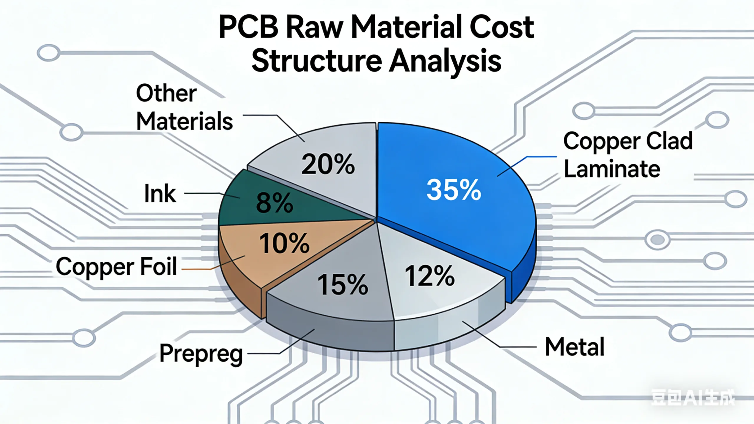
я. Деконструкция стоимости: The “Золото и Серебро” Соломинка, ломающая спину верблюду
Структура затрат на сырье печатная плата сложный, но ламинаты с золотым и медным покрытием, несомненно, являются двумя самыми тяжелыми “взвешенные акции.” Согласно анализу авторитетной отраслевой компании Prismark, в типичном многослойном виде Печатная плата для серверов, CCL может учитывать 30%-40% стоимости, в то время как драгоценные металлы, такие как золото, используются в гальваническом покрытии и отделке поверхности. (например, СОГЛАШАТЬСЯ) может составлять 8%-15%. Вместе, они приближаются к половине общей стоимости материала. Это можно упростить как:
Стоимость сырья для печатных плат ≈ (Стоимость CCL × доля) + (Стоимость драгоценных металлов × доля) + (Прочие материальные затраты)
(Источник: Призмарк Q3 2025 Отчет об анализе затрат на материалы печатных плат)
1. Золото: Больше, чем блестящий финиш
Золото в элитном сегменте печатные платы в основном используется для отделки поверхности важных соединений для обеспечения превосходной проводимости., стойкость к окислению, и паяемость. Цена цианида калия и золота (золотые соли), например, стал отраслевым барометром. Данные крупного корейского Производитель печатных плат раскрывает ошеломляющую траекторию: примерно от 50,000 KRW/грамм в 2023 к 99,000 вон/грамм в третьем квартале 2025 года — почти 100% увеличивать. Это напрямую увеличивает себестоимость производства HDI PCBS и подложки микросхем с использованием таких процессов, как ENIG (Химическое никель, иммерсионное золото). Для клиентов, требующих больших объемов Сборка печатной платы, этот перенос затрат значителен.
2. Медный ламинат: Прямой проводник спроса на ИИ
Поскольку основные диэлектрические схемы несущей цепи, результативность CCL напрямую определяет итоговый результат печатные платы целостность сигнала, тепловое управление, и надежность. Серверы ИИ, высокоскоростные переключатели, и Карты-ускорители искусственного интеллекта налагают почти жесткие требования к пропускной способности данных и потерям сигнала, стимулирование взрывного спроса на высокоскоростные/высокочастотные, сверхнизкие потери (например, Ультра низкие потери, Сорта с очень низкими потерями) ламинаты.
Отзывы ведущих производителей, таких как Samsung Electro-Mechanics, сообщающие о 10%-15% годовое увеличение затрат на закупки в третьем квартале — олицетворяет эту структурную напряженность в поставках.. Это особенно актуально для высокопроизводительных ламинатов, используемых в Материнские платы для серверов с искусственным интеллектом и Печатные платы карт-ускорителей графического процессора.
II. Глубоко сидящие драйверы: Безумие искусственного интеллекта меняет карту спроса на печатные платы
Рост цен на сырье является поверхностным симптомом; основной движущей силой является глобальная цифровая и интеллектуальная трансформация, в частности, гонка вооружений в вычислительной инфраструктуре искусственного интеллекта.
1. Ролевая эволюция: От “Разъем” к “Системно-критический компонент”
Традиционно, печатные платы рассматривались как механические опоры и платформы для электрического соединения компонентов.. В эпоху ИИ, эта роль фундаментально изменилась. Архитектуры нового поколения, примером являются такие платформы, как Rubin от NVIDIA., добиваться чрезвычайно высокой пропускной способности и плотности внутренних межсоединений, создание большого количества слоев печатные платы (обычно 22+ слои) и ИЧР любого уровня технологический стандарт. Каждый след на печатная плата влияет на задержку передачи данных и энергопотребление; его конструкция и точность изготовления напрямую влияют на синергетическую эффективность между центральными и графическими процессорами., память, и ускорители. Анализ отрасли показывает, что Материнская плата сервера AI значение кратно значению стандартного сервера, с его часть печатной платы наблюдаем соответствующее увеличение технического содержания и цены.
2. Экспоненциальный рост спроса
Обучение ИИ и выводы создают конкретные и строгие Требования к печатной плате:
-
Увеличенное количество слоев: Для размещения более сложных сетей подачи электроэнергии и большего количества уровней сигнала., Материнская плата сервера AI количество слоев приближается к 30 слои и не только.
-
Улучшения материалов: Скорость передачи данных от 224 Гбит/с и выше стимулирует спрос на M6, Ламинат со сверхнизкими потерями класса М7 (Df так низко, как 0.0015).
-
Размер & Интеграция: Плата большего размера для интеграции большего количества вычислительных блоков, и продвинутые процессы, такие как встроенный компонент печатные платы для улучшения интеграции и производительности.
Согласно МПК (Ассоциация, объединяющая электронную промышленность) 2025 прогнозный отчет, мировой элитный рынок печатных плат прогнозируется, что среднегодовой темп роста рынка центров обработки данных и инфраструктуры искусственного интеллекта превысит 14% от 2024 к 2028, значительно превышает средний показатель по отрасли.
III. Скачок ценности: Путь вперед через технологическую трансформацию
Лицом к лицу “затраты на дробление,” ведущий Производители печатной платы не пассивно выдерживают, а активно продвигаются к технологическим вершинам, устранение давления посредством трансформации ценности продукта и открытия новых рынков.
1. Стратегический сдвиг в сторону портфеля высококачественных продуктов
“Достижение прибыльности за счет продуктов с высокой добавленной стоимостью” это отраслевой консенсус. Ключевые пути включают:
-
Сосредоточьтесь на усовершенствованных упаковочных материалах: Чиплеты и гетерогенная интеграция становятся тенденциями, спрос на подложки для FC-BGA (Сетка из шариков с перевернутым чипом) упаковка растет. Эти носители имеют чрезвычайно малую ширину/интервал между линиями. (до 10 мкм/10 мкм и ниже), представляют собой высокие технические барьеры, и предложить большую прибыль.
-
Сделайте ставку на интерфейсы памяти нового поколения: DRAM на основе техпроцесса 1c-нанометра, ориентируясь на коммерциализацию вокруг 2026, будет стимулировать спрос на печатные платы поддержка интерфейсов памяти DDR5 со скоростью 8 Гбит/с+. Более того, Печатные платы SoCAMM (Модуль памяти со сжатием), будущее решение памяти, специально разработанное для серверов искусственного интеллекта, представляют собой новую точку роста в дизайн печатной платы и производство.
-
Принятие волны ASIC: Собственные ИИ-чипы (ASIC-чипы) от облачных гигантов, таких как Google, Амазонка, и Microsoft стимулируют спрос на индивидуальные межсоединения высокой плотности. (ИЧР) ASIC-подложки. Эти продукты подчеркивают высокую скорость, плотность, и надежность, представляющие типичных дорогостоящих перевозчиков на переднем конце печатная плата процесс.
2. Оптимизация экономической эффективности благодаря инновациям
Простое перекладывание расходов является неустойчивым. Повышение экономической эффективности за счет технологических инноваций является основным отличием.
-
Оптимизация дизайна: Использование передовых инструментов моделирования для оптимизации дизайна макета., потенциальное сокращение количества слоев или использование более экономичных альтернатив материалов, гарантирующих при этом производительность..
-
Инновации в процессах: Совершенствование производственных процессов для увеличения использования материалов (например, Оптимизация панели CCL) и снижение толщины золота до минимально надежного стандарта (соблюдать МПК-4552/4556 спецификации).
-
Сотрудничество в цепочке поставок: Установление стратегического партнерства с поставщиками ламината и химикатов для совместной разработки индивидуальных решений по материалам, которые обеспечивают баланс между производительностью и стоимостью..
Для Р&D компании, требующие Прототипирование печатной платы и малообъемный Производство печатных плат, Выбор партнера, предлагающего комплексные услуги по проектированию, производству и сборке, а также опыта в этих высокотехнологичных сферах имеет решающее значение..
IV. Будущий перспективы: 2026, Переломный момент в изменении стоимости печатных плат
2026 широко рассматривается как поворотный год для ремоделирования стоимости в печатная промышленность. С одной стороны, Давление на стоимость сырья может частично снизиться с вводом в эксплуатацию новых мощностей. Что еще более важно, дивиденды от технологических обновлений, вызванных искусственным интеллектом, HPC (Высокопроизводительные вычисления), и высокоскоростная связь (например, 5.5Г/6Г) станет полностью очевидным.
Метрика для Стоимость печатной платы будет развиваться из “цена за квадратный метр” больше в сторону “стоимость за единицу полосы пропускания” или “стоимость одного ватта КПД.” Производители печатной платы способен предоставлять решения системного уровня с глубоким опытом в области целостности сигналов, целостность власти, и управление температурным режимом будут иметь решающее конкурентное преимущество..
Заключение: Строительство рва в эпицентре бури
Что печатная промышленность переживает это “боли роста” подпитывается высоким спросом и сопровождается глубокими технологическими изменениями. Колебания цен на золото и ламинаты — лишь наиболее заметные главы в этом великом повествовании.. Основная история в том, что печатные платы выходят из-за кулис на центральное место в электронике, их производительность напрямую определяет потолок высокопроизводительных вычислительных систем.
Для брендов электроники и R&D фирмы, сейчас самое время переоценить Стратегии закупок печатных плат и Партнеры ПКБА. Помимо цены за единицу, более глубокая оценка технических возможностей поставщика и опыта массового производства многослойных плат, высокоскоростное нанесение материала, и усовершенствованные межкомпонентные соединения имеют важное значение. Партнерство с дальновидным технологическим лидером для совместной оптимизации проектов с учетом проблем с затратами будет ключом к победе на будущих рынках..
Свяжитесь с профессиональным поставщиком печатных плат/PCBA сегодня, чтобы получить индивидуальные схемотехнические решения и точные расценки на ваш искусственный интеллект следующего поколения., центр обработки данных, или высококачественные коммуникационные продукты, и перехватить инициативу в этом технологическом всплеске.
