
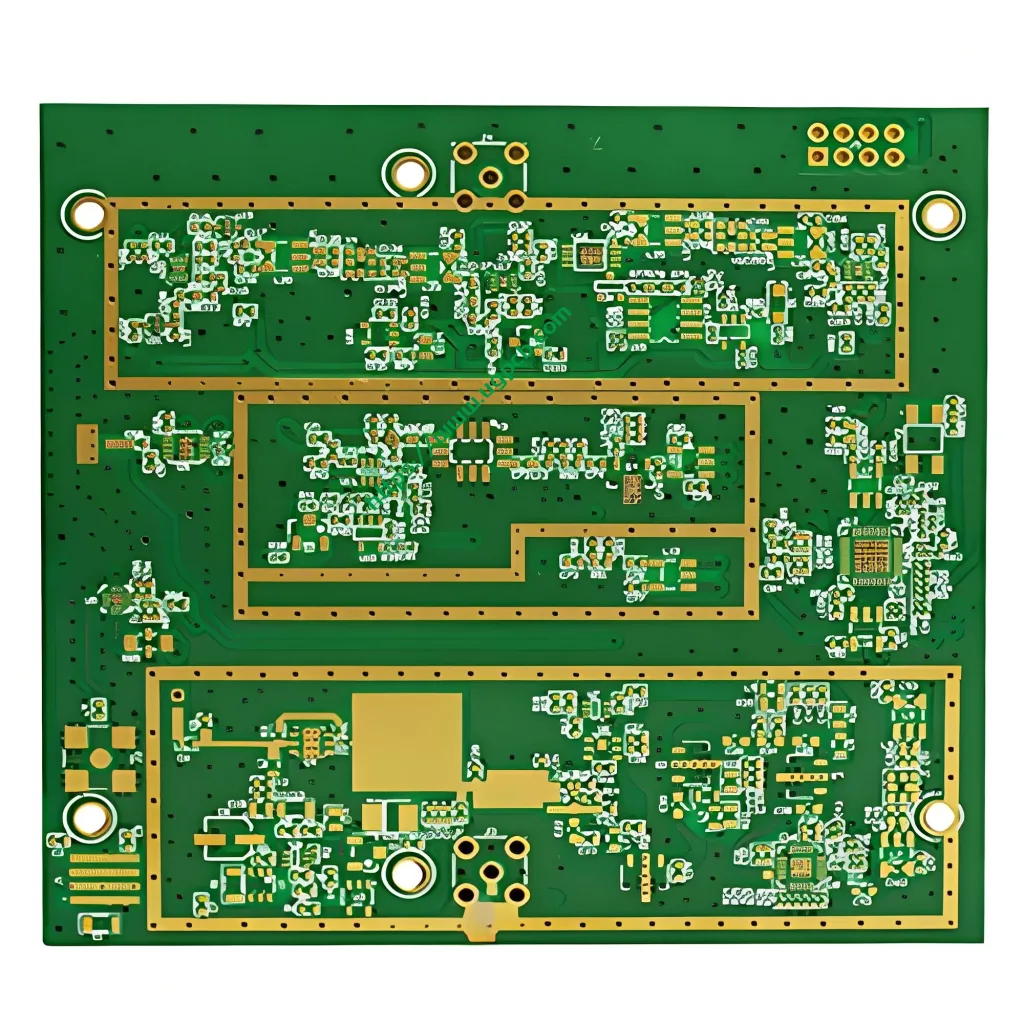
1. Определение продукта: What Is a 6-Layer Rogers + FR4 Hybrid Stacked PCB?
A 6-layer Rogers + FR4 hybrid stacked PCB is a multi-dielectric laminated circuit board. It combines Rogers high-frequency materials (typically RO4000 series) with standard FR-4 substrates in a single stack-up.
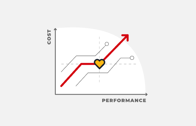
In this 6-layer PCB, Rogers layers carry high-frequency RF signals. FR4 layers handle low-speed signals, Распределение энергии, and mechanical support. Special bondply sheets bond the different materials under high temperature and pressure. For a symmetric stack-up where Rogers sits on the outer layers and FR4 on the inner layers, the hybrid solution saves 30% к 50% material cost compared to a full-Rogers design. В то же время, RF performance remains almost the same.
2. Научная классификация & Naming Standards
This product falls under the following industry-standard categories:
- By material structure: Mixed dielectric high-frequency PCB
- По количеству слоев: 6-layer rigid multilayer board
- By IPC standards: МПК-6012 (Rigid Printed Boards) / МПК-4103 (High-Frequency Base Materials)
- By application: 5G base station power amplifier module
- By process feature: Hybrid lamination / hybrid pressing PCB
3. Ключевые параметры & Материальные спецификации
3.1 Субстрат: Роджерс + FR4 Гибрид
This 6-layer hybrid stacked PCB uses Rogers hydrocarbon ceramic materials (RO4350B is the most common type) combined with FR4. РО4350Б complies with IPC-4103 for high-speed and high-frequency base materials. It can be processed on standard FR4 production lines.
The table below shows key electrical properties from the Rogers official data book:
| Материал | Dk @ 10GHz | Df @ 10GHz | Тг (°С) | UL 94 Воспламеняемость | Теплопроводность (W/m · k) |
|---|---|---|---|---|---|
| РО4350Б | 3.48 ±0,05 | 0.0037 | >280 | В-0 | 0.62 |
| РО4003C | 3.38 ±0,05 | 0.0027 | >280 | Н/Д | 0.71 |
| РО4835 | 3.48 ±0,05 | 0.0037 | >280 | В-0 | 0.66 |
Data source: Rogers RO4000 Series Data Sheet
The FR4 part uses a high-Tg reinforced laminate (Тг >= 170°C) according to IPC-4101/126. This meets the thermal cycling stability required for communication equipment.
3.2 Толщина меди & Толщина доски
- Толщина меди: 1 унция (35 мкм) finished copper on all signal, власть, и грунтовые слои.
- Total board thickness: 2.3 мм. This thickness balances mechanical rigidity, lamination stability, and heat spreading for high-current networks.
3.3 Припаяя маска & Шелковик
- Спорная маска цвет: Зеленый (настраиваемый)
- Silkscreen color: Белый (настраиваемый)
3.4 Surface Finish – ENIG (Химическое никель, иммерсионное золото)
This 6-layer PCB uses ENIG as the final surface finish. The nickel layer provides a diffusion barrier and mechanical protection. The gold layer ensures solderability, стойкость к окислению, and low contact resistance. ENIG also tolerates multiple reflow cycles. For high-frequency channels, the smooth surface reduces skin-effect losses.
3.5 Outer Layer Trace Width / Spacing
The outer layer design uses7 mil trace width and 7 mil spacing (приблизительно. 178 мкм / 178 мкм). This choice meets several needs:
- Достигает 50 Ohm characteristic impedance for RF signals on the 6-layer hybrid stack-up.
- Matches the high-yield window for pattern transfer in mainstream PCB manufacturing.
- Provides enough copper peel strength and current-carrying capacity.
4. Stack-Up Structure & Design Principles for 6-Layer PCBs
Stack-up design is the core of hybrid medium Производство печатных плат. According to IPC-2221B, a 6-layer hybrid stack-up must follow these principles.
4.1 Symmetry Principle (Low Warpage)
This product uses a symmetric stack-up: Слой 1 and Layer 6 are Rogers materials (carrying RF microstrip signals). Слои 2 к 5 are FR4 (containing full ground planes, power planes, and low-speed control traces).
A symmetric stack-up balances thermal stress during high-temperature lamination and reflow soldering. Warpage stays below 0.6% in typical production lines. A non-symmetric design can reach warpage above 1.2%.
4.2 Signal – Reference Plane Adjacency (RF Signal Integrity)
The high-speed RF signal layer (Слой 1) sits directly next to a solid ground reference plane (Слой 2). This forms a microstrip or coplanar waveguide structure. Return current follows the shortest path, which reduces loop inductance and radiated EMI.
In this 6-layer PCB, every signal layer has an adjacent complete copper plane. This suppresses crosstalk and improves EMI immunity.
4.3 Power – Ground Plane Pairing (Low PDN Impedance)
Слой 3 and Layer 4 act as the power distribution plane and the main ground plane, соответственно. They are tightly coupled. By controlling the dielectric thickness between them within the 2.3mm board, the power distribution network (ПДН) impedance can drop to tens of milliohms. This supports the transient current demands of a power amplifier (А) transistor.
4.4 Совместимость процессов & Контроль импеданса
According to IPC-2221, typical impedance tolerance for high-speed PCBs is +/-5%. Precision high-frequency microwave designs or 100Gbps+ digital interconnects may require +/-3%. This product targets the +/-5% tolerance for validation.
5. Принцип работы: Electromagnetic Signal Transmission in a Mixed Dielectric
5.1 RF Signal Propagation
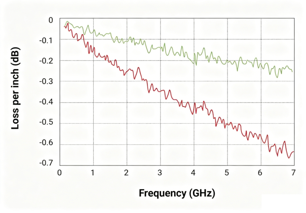
In this 6-layer Rogers+FR4 hybrid PCB, high-frequency microwave signals travel inside microstrip or stripline structures on the Rogers dielectric. Rogers material has an ultra-low dissipation factor (Df = 0.0037 for RO4350B at 10GHz) and a stable dielectric constant (Dk = 3.48 +/-0.05). Как результат, signal attenuation at GHz frequencies is much lower than on FR4.
For a microstrip line on RO4350B, the insertion loss at 28GHz is approximately 0.4 дБ/дюйм. Standard FR4 material at the same frequency shows more than 1.2 дБ/дюйм.
5.2 Signal Integrity in a Hybrid Medium
The hybrid stack-up uses a material segregation strategy. High-frequency sensitive signals run on Rogers layers (outer or inner with low-loss dielectric). Power distribution and digital control use FR4 inner layers. This approach greatly reduces cost compared to a full-Rogers design. To avoid reflections and timing errors at the boundary between different dielectric constants, engineers must precisely calculate the dielectric thickness, Ширина следа, and reference plane spacing. Then they verify the design with TDR impedance testing.
6. Приложение: Power Amplifiers in the Communication Industry
This 6-layer гибридная печатная плата is designed specifically forусилители мощности (Нет) in thecommunication industry. Typical use cases include:
- 5G macro and small cell base stations (ВЧ-модули внешнего интерфейса) : PA output power in Sub-6GHz and mmWave bands often exceeds 30W. Macro base station PAs can reach above 50W. The board must provide both low-loss RF paths and reliable heat dissipation.
- Massive MIMO antenna arrays: The high-frequency substrate must host multiple transceiver (TR) components and control circuits. The 6-layer hybrid structure separates RF and digital sections efficiently.
- Активные антенные блоки (AAUs) and small cells: These require a balance of signal integrity and power integrity. The hybrid 6-layer design meets dense routing requirements through optimized layer function assignment.
The core advantage is clear: Rogers layers provide ultra-low loss for RF signals, while inner FR4 layers carry DC power and control logic for GaN/GaAs PA transistors. This keeps overall insertion loss and thermal resistance within the strict limits of communication PAs.
7. Product Performance: Электрический, Термальный & Reliability Metrics
7.1 RF Electrical Performance
- Dielectric constant stability: RO4350B has a typical Dk of 3.48 at 10GHz with a tolerance of +/-0.05. It also maintains good temperature stability from -50°C to 150°C (TCDk ≈ 50 ppm/° C.).
- Коэффициент рассеяния: Дф <= 0.004 from 3.5GHz to 28GHz. This ensures RF channel insertion loss meets 5G requirements. Например, at 28GHz, Df = 0.0037 gives much lower loss than a standard FR4 board of the same thickness.
- Контроль импеданса: With 7/7mil trace/space and proper dielectric thickness and reference plane layout, the board achieves 50 Ohm +/-10% импеданс. This matches the RF port requirements of standard communication modules.
7.2 Тепловые характеристики
- Теплопроводность: RO4350B provides 0.62 W/m · k, better than standard FR4. This helps spread heat from PA hot spots through copper vias and pads.
- Температура стеклянного перехода: Rogers material has Tg > 280°С. The high-Tg FR4 inner layers have Tg >= 170°C. This ensures rigidity over a wide temperature range and provides good reflow soldering margin.
7.3 Reliability Indicators
- Flammability rating: RO4350B is UL 94 В-0 проверенный, meeting communication equipment safety standards.
- Moisture absorption: RO4350B has moisture absorption <= 0.06%. Electrical performance remains stable in humid environments.
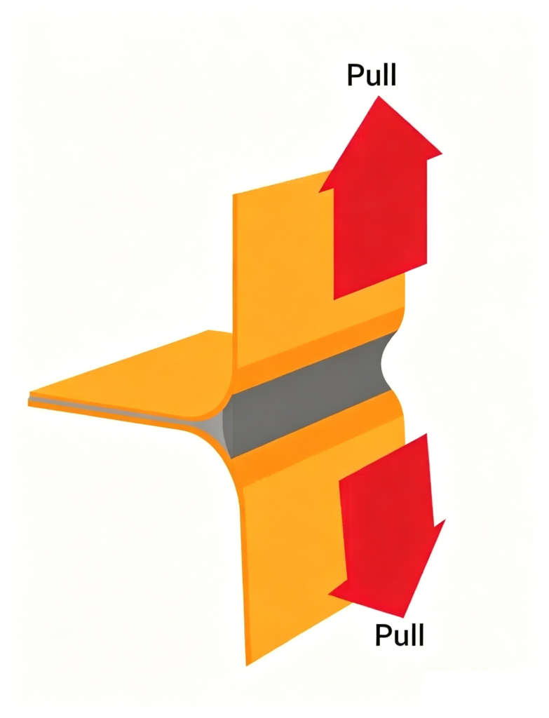
- Lamination adhesion: A dedicated bondply (например, РО4450F) ensures a strong bond between Rogers and FR4. Thermal cycle tests show no delamination.
- Производство печатных плат & инспекция: This product is manufactured and accepted according to IPC-6012. All key performance indicators are fully or sample-tested before shipment.
8. Структурные особенности
①Hybrid dielectric separation: RF signal layers use low-loss Rogers. The remaining layers use high-Tg FR4. This gives a precise trade-off between performance and cost.
②Fully symmetric stack-up: L1 and L6 are Rogers. L2 to L5 are FR4. Symmetry minimizes warpage.
③Embedded power and ground planes: Full copper inner planes provide low-impedance paths and EMI shielding.
④Thick board design (2.3мм) : Provides structural rigidity and thermal mass for high-power PA devices.
⑤High-precision outer layer pattern: 7/7mil trace/space enables accurate 50 Ohm RF transmission lines.
⑥ЭНИГ обработка поверхности: The flat, low-roughness pad surface minimizes skin-effect losses at high frequencies while ensuring solderability and contact reliability.
9. Производственный процесс: 8 Key Steps
① Material preparation & incoming inspection – Check Rogers high-frequency laminates and FR4 cores against IPC-4103 and IPC-4101.
② Inner layer imaging (L2 to L5) – Use LDI exposure and alkaline etching to form power planes, основные плоскости, and control traces on FR4 cores.
③ Inner layer AOI & oxide treatment – Perform automatic optical inspection and then black oxide / brown oxide treatment to improve lamination adhesion.
④ Hybrid lamination prep & нажатие – Stack Rogers cores, bondply, and FR4 inner layers alternately according to the stack-up. Laminate under high temperature and pressure. Typical lamination temperature: 190°C to 218°C. Pressure: 200 к 300 пси (приблизительно. 14 к 21 bar).
⑤ Drilling & metallization – Drill through-holes with high-quality tungsten carbide bits. Then perform desmear, Химическое осаждение меди, and panel plating to create layer-to-layer connections. Some critical ground vias may be resin-plugged.
⑥ Outer layer imaging (L1 and L6) – Expose, develop, and etch to form 7/7mil RF microstrip lines.
⑦ Solder mask & legend – Apply green solder mask ink over the whole board. Cure at high temperature and then screen-print white legend.
⑧ Surface finish – ENIG – Deposit 0.05~0.1μm gold over 3~5μm nickel on the circuit pads. Окончательно, perform electrical testing and final inspection, then vacuum-pack for shipment.
During the special process of hybrid lamination, control the ramp rate, давление, and bondply material matching carefully. This ensures a dense, void-free bond between different dielectrics.
10. Why Choose UGPCB’s 6-Layer Rogers+FR4 Hybrid High-Frequency PCB?
❶17+ years of RF PCB manufacturing experience – UGPCB has over 10 years of experience in высокочастотная печатная плата development and production in China. We have mature process control for Rogers+FR4 hybrid lamination.
❷Cost saving of 30% или больше – By using Rogers only on critical RF layers and FR4 elsewhere, we save at least 30% material cost compared to a full-Rogers design.
❸UL 94 В-0 and IPC compliance – We use RO4350B with V-0 rating and high-Tg FR4. This meets fire safety requirements for communication base stations and industry quality systems.
❹One-stop service – UGPCB handles everything from Gerber design review, hybrid stack-up process simulation, sample prototyping, to mass production. This reduces supply chain communication overhead.
❺100% electrical testing and impedance verification – We use Летающий зонд or fixture testing for all boards. We perform TDR testing on critical impedance lines to ensure the product matches the design expectations.
11. How to Request a Quote?
Engineers, procurement specialists, и р&D managers are welcome to submit an RFQ to UGPCB. If you need 6-layer Rogers+FR4 hybrid PCBs or similar high-frequency PCBA manufacturing services, please contact us as follows:
- Submit Gerber files, a PCB specification sheet (including 2.3mm thickness, 1Оз меди, ENIG finish), and your target impedance requirements.
- Specify your application (communication power amplifier) and volume requirements.
Request a quote now – UGPCB will provide fast engineering review and competitive volume pricing. Our technical support team will help you with hybrid stack-up design review. We will help you achieve the best balance between high-frequency performance and mass production manufacturability.
Important Note: The Rogers RO4000 series electrical properties (Дк, Дф, Тг, теплопроводность, и т. д.) cited in this document come from the Rogers official data sheet. References to IPC-2221B, МПК-6012, МПК-4103, and other IPC standards are based on publicly available IPC technical literature. All data should be verified against the original manufacturer and IPC published documents as the final reference.


