


я. Обзор продукта
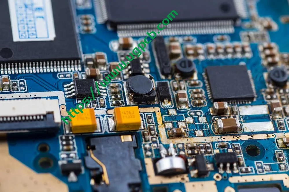
Двухсторонняя печатная плата UGPCB со сквозными отверстиями представляет собой высокопроизводительную двухслойную жесткую плату. печатная плата построен на стеклоэпоксидной подложке FR-4 с использованием металлизированных сквозных отверстий (ПТХ) технология. Правление измеряет 86.9 × 73.58 мм толщиной 1.0 мм, толщина медной фольги 1/1 ОЗ (35 мкм как на внешнем, так и на внутреннем слоях), и бессвинцовая пайка горячим воздухом для выравнивания (ХАСЛ) обработка поверхности. Паяльная маска зеленая., и легенда шелкографии белая.
Двусторонняя печатная плата со сквозными отверстиями (двусторонняя печатная плата) имеет проводящую схему на обеих сторонах изолирующей подложки, с металлизированными сквозными отверстиями, обеспечивающими электрическое соединение между двумя слоями. По сравнению с односторонними печатными платами, двусторонние печатные платы обеспечивают на 60–80 % большую плотность разводки и поддерживают более сложные схемы.. УГКПБ, опирается на сертифицированные по ISO системы качества и производственные процессы, соответствующие требованиям IPC., поставляет высококачественные двусторонние печатные платы со сквозными отверстиями и готовые к использованию печатная плата услуги производителям электроники по всему миру.
II. Определение продукта и технические характеристики
Согласно IPC-6012F Квалификационные и эксплуатационные характеристики жестких печатных плат (опубликовано в сентябре 2023), Двусторонняя печатная плата со сквозными отверстиями классифицируется как жесткая печатная плата с металлизированными сквозными отверстиями. (Тип 2). Его основной особенностью является электрическое соединение между проводниками с обеих сторон через стенки отверстий с медным покрытием.. UGPCB производит этот продукт в полном соответствии со стандартом IPC-6012F и соответствует классу 2 Требования к производительности (специальное сервисное электронное оборудование).
Ключевые спецификации:
| Параметр | Спецификация |
|---|---|
| Материал подложки | ФР-4 (Огнестойкий UL 94 В-0) |
| Количество слоев | 2 слои (двусторонний) |
| Толщина доски | 1.0 мм |
| Размеры платы | 86.9 × 73.58 мм |
| Минимальный диаметр отверстия | 0.236 мм |
| Минимальная ширина линии / Расстояние | 0.32 × 0.37 мм |
| Медная толщина фольга | 1/1 ОЗ (приблизительно. 35 мкм с каждой стороны) |
| Поверхностная отделка | Бессвинцовый HASL (Выравнивание припоя горячего воздуха) |
| Припаяя маска / Легенда | Зеленая паяльная маска / Белая шелкография |
III. Рекомендации по проектированию
3.1 Выбор материала подложки — инженерная ценность FR-4
ФР-4 — это обозначение класса огнестойкости, установленное Национальной ассоциацией производителей электротехники. (НЕТ). Буквы “фр.” стенд для огнестойких, и число “4” обозначает систему из эпоксидной смолы, армированную стеклотканью.. Для МПК-4101 Спецификация базовых материалов для жестких и многослойных печатных плат, FR-4 класса A1 представляет собой основной уровень производительности с оптимальной механической прочностью., электрические свойства, и долговременная надежность.
Ключевые показатели эффективности FR-4 (Источник: IPC-4101 и отраслевые стандарты):
-
Температура стеклянного перехода (Тг): 130–140°С (стандартный ФР-4)
-
Диэлектрическая проницаемость (Дк) @ 1 ГГц: 4.2–4,5
-
Коэффициент рассеяния (Дф) @ 1 ГГц: ≤ 0.020
-
Рейтинг воспламеняемости: UL 94 В-0
-
Водяной поглощение (24 часы): ≤ 0.10%
FR-4 остается преобладающим материалом подложки в индустрии печатных плат, поскольку он обеспечивает превосходный баланс механической прочности., электрическая изоляция, стабильность размеров, и технологичность.
3.2 Стандарты проектирования схем согласно IPC-2221
Для МПК-2221 Общий стандарт проектирования печатных плат, При расчете ширины проводника необходимо учитывать допустимую токовую нагрузку., повышение температуры, и толщина меди. Формула допустимой нагрузки по току IPC-2221::
Я = k · ΔT^0,44 · A^0,725
Где:
-
I = максимальная допустимая нагрузка по току (А)
-
k = эмпирическая константа (0.048 для внешних слоев, 0.024 для внутренних слоев)
-
ΔT = допустимое повышение температуры (°С)
-
A = площадь поперечного сечения проводника (мил²), где А = W × Т
Продукция UGPCB имеет ширину линии 0.32 мм (приблизительно. 12.6 мил), межстрочный интервал 0.37 мм (приблизительно. 14.6 мил), и толщина меди 1 ОЗ (35 мкм). Для трассы внешнего слоя при повышении температуры на 10°C:
А = 0.32 мм × 0.035 мм = 0.0112 мм² ≈ 17.36 мил²
Я = 0.048 × 10^0,44 × 17,36^0,725 ≈ 0.048 × 2.75 × 7.82 ≈ 1.03 А
Эта ширина проводника поддерживает примерно 1 тока, удовлетворение потребностей в мощности и передаче сигналов большинства бытовой электроники и промышленного оборудования управления. IPC-2221 рекомендует ограничить максимальное повышение температуры до 10°C или 20°C, чтобы продлить срок службы печатной платы..
3.3 Диаметр отверстия и соотношение сторон
Соотношение сторон сквозного отверстия является важнейшим показателем для оценки сложности сверления и металлизации отверстия.. Формула:
Соотношение сторон = толщина платы / Диаметр просверленного отверстия
Для продукции УГКПБ с 1.0 Толщина доски мм и 0.236 мм минимальный диаметр отверстия:
Соотношение сторон = 1.0 / 0.236 ≈ 4.24:1
Это соотношение сторон значительно ниже рекомендованного в отрасли верхнего предела. 10:1 и консервативный расчетный порог 8:1. Это указывает на низкую сложность сверления и металлизации., высокие показатели доходности, контролируемые затраты, и гарантированная сквозная надежность.
3.4 Справочник по проектированию рельефа местности
Для МПК-7351 Общие требования к конструкции поверхностного монтажа и стандарту схемы расположения опор, Конструкция контактной площадки должна обеспечивать адекватное формирование галтелей припоя и обеспечивать возможность пайки., проверяемость, и требования к перерабатываемости. Для сквозных компонентов, диаметр фаски обычно рекомендуется составлять в 1,8–2,2 раза больше диаметра отверстия, чтобы обеспечить достаточную ширину кольцевого кольца..
IV. Принцип работы
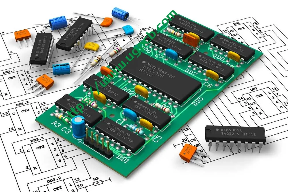
Двусторонняя печатная плата со сквозными отверстиями работает по трем основным технологиям.:
1. Двусторонняя маршрутизация — Узоры проводящих цепей выгравированы как на верхней, так и на нижней поверхностях изолирующей подложки FR-4., возможность размещения компонентов с обеих сторон. Это значительно увеличивает плотность схемы и гибкость конструкции..
2. Позолоченное сквозное отверстие (ПТХ) Соединение — После сверления, Химическое осаждение меди и электролитическое меднение создают проводящий слой на стенках отверстий.. Это создает низкоомное сопротивление, высоконадежные электрические соединения между верхним и нижним слоями. По классу IPC-6012F 2, минимальная средняя толщина медного покрытия на стенках отверстий должна быть ≥ 20 мкм.
3. Сборка компонентов и пайка — Компоненты монтируются через отверстие (ТТТ) или поверхностного монтажа (СМТ) технологии и электрически соединены посредством пайки оплавлением или волновой пайкой., производство полнофункциональной печатной платы (Печатная плата в сборе) модуль.
В. Классификация продуктов
Согласно системе классификации жестких печатных плат IPC-6012F., Продукция УГКПБ классифицируется следующим образом::
| Классификация Измерение | Категория |
|---|---|
| По конструкции | Жесткая печатная плата с металлизированными сквозными отверстиями, Двусторонний (Тип IPC-6012F 2) |
| По классу производительности | Сорт 2 (Электронное оборудование для специального обслуживания) |
| По материалу подложки | FR-4 Эпоксидный стеклотканевый ламинат (МПК-4101/21) |
| По количеству слоев | 2-Слойная доска |
| По отделке поверхности | Бессвинцовый HASL |
| По классу воспламеняемости | UL 94 В-0 |
По домену приложения, этот продукт попадает в категорию Двухсторонняя печатная плата общего промышленного класса категория, подходит для бытовой электроники, промышленное управление, оборудование связи, силовые адаптеры, и другие приложения средней надежности.
VI. Материальная композиция
6.1 Подложка — ламинат, плакированный медью, FR-4.
FR-4 — это армированный стекловолокном эпоксидный ламинат, состоящий из тканого стеклоткани электронного качества в качестве армирования и эпоксидной смолы в качестве связующего., консолидируется под воздействием высокой температуры и давления. Это UL 94 В-0 Класс воспламеняемости означает, что при испытании на вертикальное горение, материал самозатухает внутри 10 секунд после каждого из двух 10-секундных применений пламени, без горящих капель, воспламеняющих хлопок.
6.2 Медная фольга — 1/1 ОЗ
Одна унция (1 ОЗ) медная фольга имеет толщину 35 мкм (1.37 мил). УГКПБ использует 1 Медь OZ на обоих внешних слоях (назначенный 1/1 ОЗ), обеспечение одинаковой токовой способности и проводимости с обеих сторон.
6.3 Поверхностная обработка — бессвинцовый HASL
Бессвинцовый HASL предполагает погружение печатной платы в расплавленный бессвинцовый припой. (обычно Sn-Cu, Sn-Cu-Ni, или сплавы Sn-Ag-Cu), затем с помощью ножей горячего воздуха под высоким давлением выровняйте и удалите излишки припоя.. Это дает однородный, паяемое защитное покрытие на медных поверхностях. Процесс соответствует требованиям IPC-6012F и экологическим директивам RoHS..
6.4 Паяльная маска и легенда
-
Зеленая паяльная маска — Охватывает все области схемы, кроме контактных площадок, обеспечение изоляции, защита от окисления, и предотвращение короткого замыкания.
-
Легенда белой шелкографии — Идентифицирует ссылочные обозначения компонентов., маркеры полярности, номера деталей платы, и уровни редакций для облегчения сборки и отладки.
VII. Производительность продукта
7.1 Электрические характеристики
| Параметр производительности | Ценить | Справочный стандарт |
|---|---|---|
| Диэлектрическая проницаемость (Дк) @ 1 ГГц | 4.2–4,5 | МПК-4101 |
| Коэффициент рассеяния (Дф) @ 1 ГГц | ≤ 0.020 | МПК-4101 |
| Сопротивление изоляции | ≥ 10^12 Ом | МПК-6012Ф |
| Диэлектрическое выдерживаемое напряжение | По диэлектрической прочности | МПК-6012Ф |
7.2 Механические характеристики
| Параметр производительности | Ценить | Справочный стандарт |
|---|---|---|
| Толщина доски | 1.0 мм ± 10% | МПК-6012Ф |
| Прочность меди на отслаивание | ≥ 1.1 N/мм | МПК-6012Ф |
| Рейтинг воспламеняемости | UL 94 В-0 | Стандарт УЛ |
| Тг (Температура стеклянного перехода) | 130–140°С | МПК-4101 |
7.3 Надежность
По классу IPC-6012F 2 требования, продукт должен пройти следующие проверки надежности:
-
ТЕПРЕСКИЙ СТРАНТ -Тест (288°С, 10 секунды, без расслаивания и вздутий)
-
Испытание на адгезию медных сквозных отверстий с покрытием (минимальная средняя толщина меди стенки отверстия ≥ 20 мкм)
-
Тест на паяемость
-
Проверка электрической целостности и сопротивления изоляции
VIII. Структура продукта
Двусторонняя печатная плата UGPCB со сквозными отверстиями имеет симметричную двухслойную конструкцию.. Сверху вниз:
-
Верхний слой легенды (Белый шелкография)
-
Верхний слой паяльной маски (Зеленые чернила)
-
Верхний слой медной фольги (1 ОЗ, 35 мкм)
-
Изоляционная подложка FR-4 (1.0 ММ толщина)
-
Нижний слой медной фольги (1 ОЗ, 35 мкм)
-
Нижний слой паяльной маски (Зеленые чернила)
-
Нижний слой легенды (Белый шелкография)
-
Покрытые сквозные отверстия (ПТХ) — Охватывают всю толщину платы благодаря медным стенкам отверстий, обеспечивающим межслойное соединение.
IX. Особенности продукта
-
Высокая плотность маршрутизации — Двусторонняя разводка обеспечивает на 60–80 % большую плотность, чем односторонние платы., поддержка более сложных схем.
-
Высоконадежное сквозное соединение — Металлизированное сквозное отверстие (ПТХ) технология обеспечивает долговременную электрическую надежность между слоями, с толщиной медной стенки отверстия, соответствующей классу IPC-6012F 2 требования (≥ 20 мкм в среднем).
-
Отличная огнестойкость — Подложка FR-4 соответствует требованиям UL 94 В-0 Рейтинг воспламеняемости, обеспечение безопасности в нештатных условиях эксплуатации.
-
Не содержит свинца и экологически чистый — Бессвинцовая поверхность HASL соответствует экологическим директивам RoHS..
-
Возможности схемы с мелким шагом — Минимальная ширина линии 0.32 мм и минимальное расстояние 0.37 мм вмещает средний размер- для схемотехники высокой плотности.
-
Превосходная стабильность размеров — Низкое водопоглощение FR-4 (≤ 0.10%) обеспечивает минимальное изменение размеров во влажной среде, сохранение точности сборки.
-
Зрелый производственный процесс - С 1.0 Толщина доски мм и 0.236 мм минимальный диаметр отверстия, соотношение сторон только 4.24:1 обеспечивает зрелые процессы, высокая доходность, и короткие сроки выполнения.
Х. Схема производственного процесса
Стандартный процесс производства двусторонних печатных плат UGPCB со сквозными отверстиями.:
1. Входной контроль материалов → Проверьте толщину медного ламината FR-4., качество медной фольги, и визуальные дефекты.
2. Резка → Разрезать крупноформатный ламинат, плакированный медью, по размеру рабочей панели. (86.9 × 73.58 мм).
3. Бурение → Используйте высокоточные сверлильные станки с ЧПУ для сверления всех сквозных отверстий в соответствии с файлом сверла Gerber. (минимальный диаметр 0.236 мм).
4. Позолоченное сквозное отверстие (ПТХ) → Нанесите тонкий затравочный слой меди на стенки отверстий методом химического осаждения меди..
5. Панельное покрытие → Нанесите медь электролитическим способом для наращивания меди на стенках отверстий и на поверхности до заданной толщины. (1 ОЗ).
6. Перенос узора → Ламинат сухая пленка, разоблачать, И развивайтесь, чтобы сформировать сопротивление шаблону схемы.
7. Офорт → Вытравите незащищенную медь, чтобы сформировать окончательный рисунок схемы..
8. зачистки → Удалите сухую пленку резиста со дорожек цепи..
9. Прикладная маска → Нанесите зеленые чернила для паяльной маски., разоблачать, и разверните, чтобы обнажить подушечки.
10. Поверхностная отделка → Бессвинцовый HASL.
11. Печать легенд → Легенда, нанесенная белой шелкографией.
12. Маршрутизация / V-образный вырез → Фрезерование на станке с ЧПУ до окончательного контура платы.
13. Электрические испытания → Испытание летающего щупа или приспособления для проверки целостности обрыва/замыкания.
14. Окончательный контроль качества (FQC) → Визуальный осмотр, размерная выборка, и упаковка для отправки.
XI. Сценарии приложения
UGPCB Двухсторонние печатные платы FR-4 со сквозными отверстиями, с их сбалансированной производительностью и зрелыми процессами, широко используются в:
11.1 Бытовая электроника
-
Силовые адаптеры и зарядные устройства
-
Платы управления бытовой техникой
-
Устройства умного дома
11.2 Промышленный контроль
-
Программируемые логические контроллеры ПЛК
-
Промышленные силовые модули
-
Приборы и счетчики
11.3 Коммуникационное оборудование
-
Маршрутизаторы и коммутаторы
-
Коммуникационные модули
-
Устройства преобразования сигналов
11.4 Автомобильная электроника
-
Бортовые зарядные устройства
-
Модули управления кузовом (некритичный с точки зрения безопасности)
-
Информационно -развлекательные системы
11.5 Медицинские устройства
-
Вспомогательные платы монитора пациента
-
Портативное медицинское оборудование (Сорт 2 применимый)
XII. Преимущества продукта и руководство по выбору
12.1 Почему стоит выбрать двусторонние печатные платы со сквозными отверстиями UGPCB?
-
Управление процессами, соответствующее требованиям IPC — От выбора материала до готовой продукции, полное соответствие IPC-6012F, МПК-4101, и другие международные стандарты.
-
Высокоточное производство — Минимальный диаметр отверстия 0.236 мм и минимальная ширина линии 0.32 мм соответствует среднему- требованиям дизайна высокой плотности.
-
Экологическое соответствие — Бессвинцовая поверхность HASL соответствует требованиям RoHS. 2.0 директивы.
-
Проверенная надежность — Субстрат FR-4 проверен на рынке на протяжении десятилетий и имеет стабильные характеристики..
-
Быстрая доставка — Стандартные спецификации снабжены достаточным количеством сырья., обеспечение надежных сроков выполнения заказов.
12.2 Справочник по выбору
Двухсторонние печатные платы UGPCB со сквозными отверстиями — идеальный выбор, если ваш проект соответствует этим критериям.:
-
Умеренная сложность схемы, 2 слои могут вместить
-
Рабочая частота ниже 1 ГГц (FR-4 превосходно работает в этом диапазоне.)
-
Длительная рабочая среда не превышает 120°C.
-
Экономически чувствительные приложения, требующие высокой стоимости
XIII. Запросить цену
UGPCB стремится предоставлять высококачественные услуги по производству печатных плат и услуги по производству печатных плат «под ключ» клиентам по всему миру.. Нужны ли вам двусторонние печатные платы со сквозными отверстиями стандартной спецификации или индивидуальные требования (специальная толщина доски, медная гиря, обработка поверхности, контроль импеданса, и т. д.), Команда экспертов УГКПБ обеспечивает полную поддержку от инженерного проектирования до серийного производства..
Получите предложение сегодня:
-
Отправьте файлы Gerber + технические характеристики — получите ценовое предложение в течение 24 часы
-
Поддержка от прототипа до крупносерийного производства
-
Бесплатный дизайн для производства (DFM) обзор
Контакты УГКПБ:
📧 Запросы на продажу: [sales@ugpcb.com]
🌐 Сайт: [www.ugpcb.com]
XIV. Декларация источника данных
Стандарты и данные, приведенные в этом документе, получены от следующих авторитетных организаций.:
-
МПК (Ассоциация, объединяющая электронную промышленность): МПК-6012Ф Квалификационные и эксплуатационные характеристики жестких печатных плат (Сентябрь 2023); МПК-4101 Спецификация базовых материалов для жестких и многослойных печатных плат; МПК-2221 Общий стандарт проектирования печатных плат; МПК-7351 Общие требования к конструкции поверхностного монтажа и стандарту схемы расположения опор
-
UL (Андеррайтеры лаборатории): UL 94 Стандарт на испытания на воспламеняемость пластмассовых материалов для деталей устройств и приборов
-
НЕТ (Национальная ассоциация производителей электротехники): Определение марки материала FR-4
-
Стандартные технические данные отрасли: Диэлектрическая проницаемость ФР-4, Коэффициент рассеяния, и другие параметры свойств материала













