
eMMC PCB Package Substrate Product Overview
In today’s data-centric world, the performance and reliability of embedded storage are critical. EMMC (embedded MultiMediaCard) serves as the core storage unit in smartphones, таблетки, IoT devices, and other consumer electronics. УГКПБ, leveraging deep expertise in Взаимодействие высокой плотности (ИЧР) Производство печатных плат, offers specialized eMMC Package Substrate PCBs. Designed with HL832NS material in a 4-layer, ultra-thin configuration, this substrate is the essential platform for high-speed, stable electrical interconnection between the memory controller, NAND flash dies, и основная плата. It is the optimal solution for developing next-generation compact, high-capacity storage modules.
What is an eMMC Package Substrate PCB?
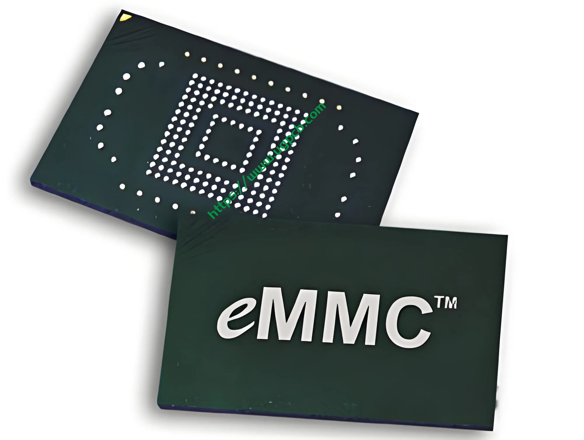
Ан eMMC Package Substrate PCB является специализированным, miniaturized печатная плата used internally within an eMMC chip package. It serves as the core interposer, providing the electrical connections and physical support between the storage controller silicon die, the NAND flash memory dies, and the external Ball Grid Array (БГА) интерфейс. Its design and manufacturing quality directly determine the signal integrity, тепловые характеристики, and overall reliability of the final eMMC module.
Основные моменты дизайна & Ключевые технические характеристики
To meet the stringent demands of eMMC chips for high bandwidth and miniaturization, UGPCB’s eMMC substrate focuses on these critical design parameters:
-
High-Density Routing: Supports ultra-fine circuitry with minimum line width/space of 20µm.
-
Micro-Via Capability: Функции minimum via diameter of 0.1mm for high-density I/O fanout.
-
Стабильное ламинирование: 4-layer construction with a controlled total thickness of 0.21mm, balancing electrical performance and mechanical strength.
-
High-Reliability Surface Finish: Мягкое золото (СОГЛАШАТЬСЯ) plating provides an oxidation-resistant, low-resistance surface for reliable wire bonding or flip-chip attachment.
-
Precise Solder Mask: PSR-4000 AUS308 solder mask offers excellent insulation and chemical resistance.
Как это работает & Структурные особенности
Как это работает: The substrate acts as the internal “нервная система” и “power grid” of the eMMC module. Its conductive traces and micro-vias route command signals from the controller to the NAND flash dies and return data. Dedicated power and ground planes ensure stable, low-noise power delivery.
Структурные особенности:
-
Ультратонкий & Компакт: 0.21mm final thickness и 11.5mm x 13mm unit size minimize space consumption.
-
Advanced Core Material: Built on HL832NS, a high-performance laminate known for excellent thermal stability and low signal loss (низкий Dk/Df), crucial for heat dissipation.
-
Multi-Layer Architecture: The 4-слой стек (typically signal, власть, земля) optimizes signal paths, reduces crosstalk, and controls impedance.
-
BGA Pad Array: The bottom side features a precise BGA pad layout for reliable surface-mount technology (СМТ) assembly of the entire module onto the host motherboard.
Primary Application & Варианты использования
Primary Application: Core interconnection platform within EMMC 5.1 and above пакеты чипов.
Типичные приложения (Варианты использования):
-
Смартфоны & Таблетки: Primary internal storage.
-
Smart TVs & Set-Top Boxes: System storage and caching.
-
IoT устройства: Умные часы, smart home hubs requiring compact embedded storage.
-
Промышленные системы управления: Embedded devices demanding high data reliability.
-
Automotive Infotainment: Storage modules meeting automotive-grade stability requirements.

Классификация & Материальная композиция
-
Классификация: Can be categorized by application grade: Consumer, Промышленный, and Automotive (this model is tailored for consumer & high-end industrial applications).
-
Material Stack-Up:
-
Core Laminate: HL832NS Высокий Тг, Low-Loss material.
-
Проводящие слои: High-purity electrolytic copper foil.
-
Припаяя маска: PSR-4000 AUS308 (Зеленый, matte/gloss optional).
-
Поверхностная отделка: Химическое никель, иммерсионное золото (СОГЛАШАТЬСЯ – Мягкое золото).
-
Преимущества производительности & Ключевые особенности
-
Превосходная целостность сигнала: Controlled impedance and low-loss HL832NS material ensure stable high-speed data transfer.
-
Высокая надежность: Stringent process controls and material selection guarantee long-term durability.
-
Effective Thermal Management: The laminate’s good thermal conductivity aids in heat dissipation from the active dies.
-
Tight Manufacturing Tolerances: 20µm line/space and 0.1mm micro-vias demonstrate передовой HDI печатная плата Производство экспертиза.
-
End-to-End Solution: UGPCB provides collaborative support from substrate design review и Изготовление печатной платы к Быстрое прототипирование PCBA.
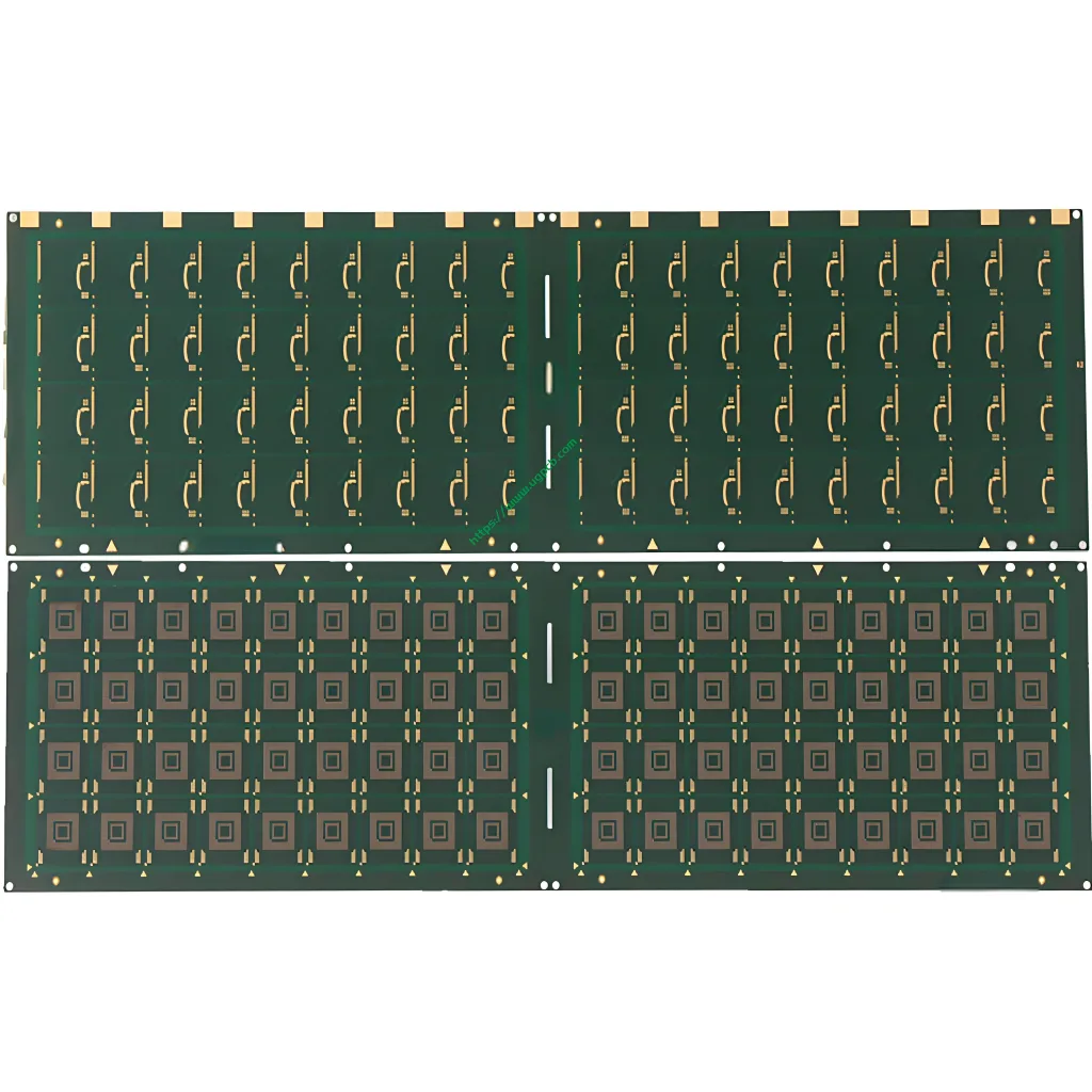
Обзор производственного процесса
Our eMMC Package Substrate manufacturing follows a stringent HDI PCB process flow:
Material Prep → Inner Layer Imaging → Lamination → Laser Drilling (0.1mm vias) → Via Metallization → Outer Layer Imaging (20µm lines) → Нанесение паяльной маски (PSR-4000) → Surface Finishing (Мягкое золото) → Electrical Testing → Routing/Scoring → Final Inspection & Упаковка.
Why Choose UGPCB for Your eMMC Package Substrate?
Choosing UGPCB means partnering with an expert in memory chip substrate manufacturing. We understand the technical evolution of storage interfaces and offer full-chain support to ensure your product excels in performance, расходы, и надежность.
Contact us today to discuss your eMMC Package Substrate requirements and request a quotation. Let UGPCB’s precision engineering be the reliable foundation for your next-generation storage solutions.


