

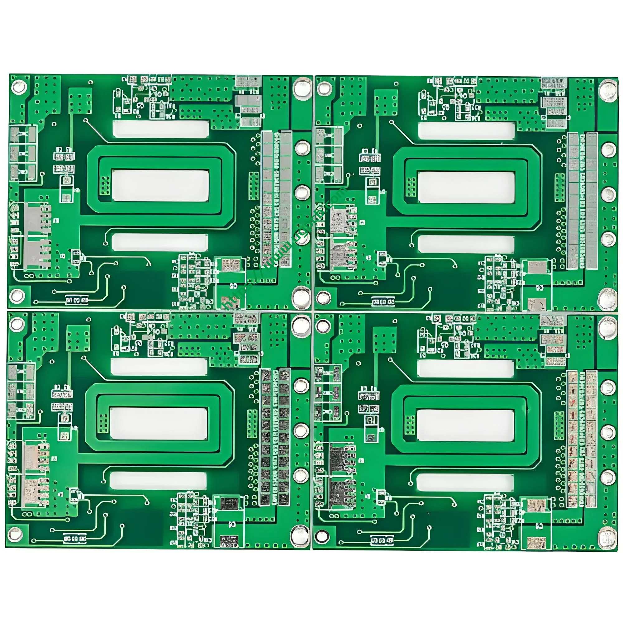
Обзор продукта: Что такое двухсторонняя печатная плата никель-палладий-золото??
Двусторонняя печатная плата никель-палладий-золото. (также известная как двусторонняя печатная плата ENEPIG) это печатная плата с химическим никелем, химическим палладием, иммерсионным золотом. (Enepic) обработка поверхности с обеих сторон доски. Эта усовершенствованная обработка поверхности основана на традиционной двусторонней структуре печатной платы за счет добавления слоя палладия между слоями никеля и золота., создание прочного трехслойного композитного покрытия, обеспечивающего превосходную паяемость, производительность склеивания проводов, и экологическая стабильность.
В двусторонней печатной плате UGPCB никель-палладий-золото в качестве основного материала используется ламинат Kingboard KB6160A FR-4 с медным покрытием.. Правление измеряет 49.6 × 32.8 мм толщиной 1.6 мм и толщиной медной фольги 1 унция (примерно 35 мкм). Паяльная маска зеленого цвета с белыми шелкографическими символами.. С минимальной апертурой 0.27 мм и минимальная ширина линий/интервал 0.27 × 0.3 мм, Эта печатная плата ENEPIG обеспечивает точность изготовления в сочетании с высококачественной обработкой поверхности..
Печатная плата никель-палладий-золото широко известна как «универсальная обработка поверхности» в электронной промышленности.. Он служит широкому спектру приложений, в том числе телекоммуникации, бытовая электроника, промышленный контроль, Системы безопасности, автомобильная электроника, питания, умные домашние устройства, Медицинское оборудование, и военные/аэрокосмические системы.
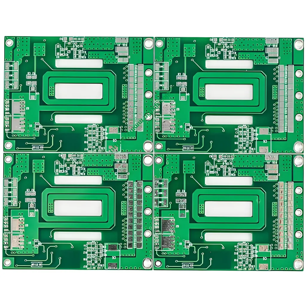
Ключевые технические характеристики
| Параметр | Спецификация |
|---|---|
| Ламинат | Кингборд KB6160A FR-4 |
| Толщина доски | 1.6 мм |
| Количество слоев | Двусторонний |
| Размер платы | 49.6 × 32.8 мм |
| Минимальная апертура | 0.27 мм |
| Минимальная ширина; | 0.27 × 0.3 мм |
| Медная толщина фольга | 1 унция (≈35 мкм) |
| Поверхностная отделка | Никель-Палладий-Золото (Enepic) |
| Припаяя маска / Легенда | Зеленая паяльная маска / Белая шелкография |
Детали ламината: KB6160A FR-4 Ламинат с медным покрытием
KB6160A — это высокопроизводительный ламинат FR-4 с медным покрытием, производимый Kingboard Laminates Holdings Ltd.. Этот материал специально разработан для стандартных двусторонних печатных плат. (PWB) Производство. Он соответствует спецификации IPC-4101/21.. Ключевые свойства включают в себя:
- УФ-блокировка (УФБ) способность: Предотвращает пропускание света во время визуализации, повышение точности и производительности переноса шаблонов
- Отличная стабильность размеров: Обеспечивает точность на протяжении всего производственного процесса.
- Превосходная термостойкость и механические свойства: Соответствует требованиям приложений с высокой надежностью
- Температура стеклянного перехода (Тг): 135°С (метод ДСК)
- Температура термического разложения (Тд): 305°С (метод ТГА)
- Z-ось Cte (A1/A2): 58 ppm/° C. (< Тг) / 286 ppm/° C. (> Тг)
- Диэлектрическая проницаемость (Дк): 4.58
- Коэффициент рассеяния (Дф): 0.022
- Объемный удельное сопротивление: 1 × 10⁸ МОм-см
- Влажно -поглощение: 0.21%
- Рейтинг воспламеняемости: UL94 В-0
(Данные выше взяты из технического паспорта Kingboard KB6160A., с методами испытаний согласно стандартам серии IPC-TM-650.)
Поверхностная обработка ENEPIG: Подробное объяснение
Что такое ЭНЕПИГ?
ENEPIG означает химический никель, химический палладий, иммерсионное золото.. Это химический метод обработки поверхности, при котором последовательно наносятся три слоя металла — никеля., палладий, и золото — на медную схему печатная плата.
Трехуровневая структура ENEPIG состоит из:
- Нижний слой – химический никель. (В): Толщина 3–5 мкм. Этот слой действует как диффузионный барьер., предотвращение миграции меди на поверхность, обеспечивая при этом механическую поддержку и основу для пайки.
- Средний слой – химический палладий. (ПД): Толщина 0,05–0,1 мкм.. Этот критический барьерный слой предотвращает взаимодействие между никелем и золотом., устранение гальванической коррозии.
- Верхний слой – иммерсионное золото (Au): Толщина 0,03–0,05 мкм.. Этот тонкий слой обеспечивает превосходную паяемость и защиту от окисления..
Согласно МПК-4556А (последний 2025 пересмотр), Требования ENEPIG к толщине отложений указаны следующим образом::
- Слой никеля: 3 мкм до 6 мкм (измерено в среднем ± 4σ)
- Палладиевый слой: 0.05 мкм до 0.30 мкм (измерено в среднем ± 4σ)
- Золотой слой: Минимум 0.030 мкм, максимум 0.07 мкм (измерено ниже среднего − 4σ)
(Приведенные выше характеристики толщины основаны на IPC-4556A., Спецификация для химического никеля/химического палладия/иммерсионного золота (Enepic) Покрытие печатных плат.)
Процесс ENEPIG
Двусторонние печатные платы UGPCB из никеля-палладия-золота изготовлены с использованием стандартизированного процесса химического нанесения покрытия.:
Обезжиривание → Микротравление → Предварительное погружение → Активация → Химическое никелирование → Химическое палладирование → Иммерсионное золочение → Сушка
Каждый этап процесса включает в себя несколько стадий промывки для обеспечения качества покрытия и адгезии.. В число химических реакций входят как окислительно-восстановительные реакции, так и реакции замещения..
Основные преимущества двусторонних печатных плат никель-палладий-золото
1. Полное устранение дефекта «Черная колодка»
ЭНИГ (Химическое никель, иммерсионное золото) Процесс уже давно страдает от дефекта «черной площадки» — состояния, при котором атака золота на слой никеля приводит к хрупкости паяных соединений и преждевременному выходу из строя.. ENEPIG решает эту проблему, вводя барьерный слой палладия между никелем и золотом., предотвращение прямого контакта и устранение зернограничной коррозии. Отраслевые данные показывают, что ENEPIG сокращает количество случаев появления черных площадок почти 90% по сравнению с ЭНИГ. В условиях экстремальных температурных циклов, ENEPIG демонстрирует до 30% более высокая надежность, чем ENIG.
2. Превосходные возможности соединения проводов
Поверхностная обработка ENEPIG обеспечивает превосходные характеристики склеивания как золотых, так и алюминиевых проводов.. Слой палладия расширяет технологическое окно для соединения золотой проволоки., обеспечение надежных проводных облигаций даже при более тонких месторождениях золота. Во многих приложениях, ENEPIG поддерживает прочность соединения проводов, превышающую 10 граммы для золотых и алюминиевых проволочных облигаций. Это делает двусторонние печатные платы никель-палладий-золото особенно подходящими для полупроводниковых корпусов и гибридных сборок, требующих соединения проводов..
3. Отличная паяемость и устойчивость к множественному оплавлению
Поверхностная обработка ENEPIG обеспечивает превосходную пайку как этилированными, так и бессвинцовыми припоями. (включая сплав SAC305). Печатные платы с покрытием ENEPIG выдерживают до 10 циклы оплавления без значительного ухудшения качества.
4. Увеличенный срок годности
Благодаря защитному палладиевому слою, Поверхностная обработка ENEPIG обеспечивает превосходную стойкость к окислению и коррозии.. Это приводит к значительно более длительному сроку хранения по сравнению с другими видами отделки поверхности.. Согласно рекомендациям МПК, Поверхностная обработка ENEPIG может соответствовать категории IPC 3 срок годности не менее двенадцати месяцев.
5. Большая гибкость дизайна
В отличие от электролитических процессов никель-золото, ENEPIG — это химический процесс, не требующий использования шин или гальванических выводов.. Это позволяет одновременно обрабатывать больше плит в одной гальванической ванне., увеличение общей пропускной способности. Кроме того, ENEPIG не накладывает ограничений на маршрутизацию., обеспечение большей гибкости при проектировании схем с высокой плотностью.
Как работают двусторонние печатные платы никель-палладий-золото
Синергетическое действие трех слоев покрытия
Исключительные характеристики двусторонних печатных плат никель-палладий-золото обусловлены точным взаимодействием трех слоев покрытия.:
① Слой никеля (Ni-P сплав) – Барьер Фонда
Слой никеля служит основой структуры ENEPIG.. Его основная функция — блокировать диффузию атомов меди к поверхности., предотвращение образования хрупких интерметаллидов Cu-Sn (IMC) при пайке или высокотемпературном воздействии. Толщина никеля обычно контролируется в пределах 3–6 мкм., содержание фосфора строго поддерживается на уровне 7–9% для баланса твердости и коррозионной стойкости..
② Палладиевый слой (ПД) – Критический барьер и уровень активации
Слой палладия является определяющей особенностью, отличающей ENEPIG от ENIG.. Он действует как «перегородка».,» предотвращение миграции и зернограничной коррозии между никелем и золотом. Слой палладия должен быть достаточно толстым, чтобы блокировать диффузию никеля к поверхности золота и предотвращать чрезмерную коррозию химического покрытия никеля..
③ Золотой слой (Au) – Защита и паяемость
Тонкий внешний слой золота защищает никель от окисления, обеспечивая при этом низкое контактное сопротивление и отличную паяемость.. Поскольку слой палладия обеспечивает изоляцию, золотой слой в ENEPIG можно сделать тоньше (0.03–0,05 мкм) без ущерба для надежности, что позволяет в некоторой степени снизить материальные затраты.
Классификация двусторонних печатных плат никель-палладий-золото
Двустороннюю печатную плату UGPCB из никель-палладия-золота можно с научной точки зрения классифицировать по нескольким параметрам.:
По количеству слоев
- Двусторонняя печатная плата: Проводящие цепи распределены по обеим сторонам подложки., с электрическими соединениями, выполненными через металлизированные сквозные отверстия (ПТХ).
Базовым материалом
- FR-4 Эпоксидный стеклотканевый ламинат: Использование Kingboard KB6160A, соответствует IPC-4101/21.
По отделке поверхности
- Enepic (Электролетное никелевое электролетное погружение палладий Золото) : Трехслойная структура композитного покрытия.
По домену приложения
- Высоконадежная печатная плата общего назначения: Подходит для телекоммуникаций, автомобильная электроника, медицинское оборудование, аэрокосмический, промышленный контроль, и еще.
По точности производства
- Прецизионная печатная плата: Минимальная апертура 0.27 мм, минимальная ширина линии/интервал 0.27 × 0.3 мм.
Схема производственного процесса
Производство двусторонних печатных плат UGPCB соответствует комплексному производственному процессу.:
Этап 1: Подготовка субстрата
- Материальная резка: KB6160A Медный ламинат разрезается по необходимым размерам..
- Бурение: Механическое сверление с минимальным отверстием 0.27 мм.
- Химическое осаждение меди & Панельное покрытие: Сквозная металлизация.
Этап 2: Формирование цепи
- Перенос узора: Сухое пленочное ламинирование → Экспонирование → Проявка.
- Травление цепей: Удаление излишков меди для формирования рисунка схемы..
- АОИ (Автоматическая оптическая проверка) : Обеспечение точности схемы.
Этап 3: Паяльная маска и легенда
- Печать паяльной маски: Нанесение зеленых чернил для защиты цепей и предотвращения образования перемычек припоем.
- Печать легенд: Белые персонажи шелкографии.
Этап 4: Поверхностная отделка (Enepic)
- Обезжиривание: Удаление поверхностных загрязнений.
- Микротравление: Легкое травление медной поверхности для улучшения адгезии..
- Предварительное погружение: Предварительная обработка перед активацией.
- Активация: Нанесение каталитического затравочного слоя палладия на медь..
- Химическое никелирование: Нанесение слоя никеля (3–5 мкм).
- Химическое палладиевое покрытие: Нанесение слоя палладия (0.05–0,1 мкм).
- Иммерсионное золотое покрытие: Нанесение золотого слоя (0.03–0,05 мкм).
- Сушка: Завершение отделки поверхности.
Этап 5: Заключительная проверка
- Электрические испытания: Обеспечение непрерывности и изоляции электрической цепи.
- Визуальный осмотр: Проверка качества поверхности.
- Упаковка & Перевозки.
Типичные приложения
Двусторонние печатные платы UGPCB никель-палладий-золото широко используются во многих отраслях промышленности.:
Телекоммуникационное оборудование
- Базовые станции, маршрутизаторы, переключатели
- Модули высокочастотной связи, РЧ устройства
Автомобильная электроника
- Блоки управления двигателем (КРЫШКА)
- Автомобильные информационно-развлекательные системы
- Адас (Расширенные системы помощи водителю)
- Бит (Системы управления батареями) для транспортных средств на новой энергии

Медицинские устройства
- Медицинские имплантируемые устройства
- Диагностические инструменты, оборудование для мониторинга пациентов
Аэрокосмическая промышленность & Оборона
- Космические аппараты и спутниковая электроника
- Системы управления авиацией
Промышленный контроль & Безопасность
- ПЛК (Программируемые логические контроллеры)
- Промышленные моторные приводы
- Оборудование безопасности и наблюдения
Бытовая электроника & Умный дом
- Материнские платы для смартфонов
- Модули управления умным домом
- Носимые устройства
Военный & Силовая электроника
- Военные электронные системы
- Силовые модули, преобразователи мощности
Почему стоит выбрать UGPCB для двусторонних печатных плат никель-палладий-золото?
✅ Соответствие стандартам IPC
Двусторонние печатные платы UGPCB из никеля-палладия-золота производятся в строгом соответствии со стандартом IPC-4556A.. Ламинат KB6160A соответствует стандарту IPC-4101/21., обеспечение полной стандартизации от основного материала до отделки поверхности.
✅ Возможности точного производства
С минимальной апертурой 0.27 мм и минимальная ширина линии/интервал 0.27 × 0.3 мм, UGPCB отвечает требованиям межсоединений высокой плотности (ИЧР) и сборка компонентов с мелким шагом.
✅ Гарантия высокой надежности
Поверхностная обработка ENEPIG уменьшает количество черных дефектов колодок почти 90% и доставляет до 30% более высокая надежность, чем ENIG, при экстремальных колебаниях температуры. Продукты выдерживают несколько циклов оплавления и соответствуют стандарту J-STD.-003 Категория 3 Требования к долговечности.
✅Профессиональная техническая поддержка
Команда УГКПБ обеспечивает полную техническую поддержку, от проверки файлов Gerber и оптимизации спецификации до сборки печатной платы.
Запросы & Заказ
Готовы превратить ваш дизайн в высококачественную двустороннюю печатную плату из никель-палладия-золота.?
📧 Электронная почта: sales@ugpcb.com
📞 Телефон: +86-135 4412 8719
🌐 Сайт: www.ugpcb.com
📋 Процесс заказа:
- Отправьте файлы Gerber, спецификация, и проектная документация.
- Инженерная группа УГКПБ выполняет DFM (Дизайн для производства) обзор.
- Подтверждение заказа и график доставки.
- Производство и контроль качества.
- Отслеживание доставки и логистики.
Нужен ли вам Прототипирование печатной платы или серийное производство, UGPCB стремится поставлять высококачественные двусторонние печатные платы никель-палладий-золото и предоставлять профессиональные технические услуги..
Декларация источника данных
Технические данные и стандартные характеристики, приведенные в этом документе, получены от следующих авторитетных организаций.:
- МПК-4556А: Спецификация для химического никеля/химического палладия/иммерсионного золота (Enepic) Покрытие печатных плат (2025 пересмотр)
- МПК-4101/21: Спецификация базовых материалов для жестких и многослойных печатных плат – лист технических характеристик, применимый к KB6160A
- Технический паспорт Kingboard KB6160A (Kingboard Laminates Holdings Ltd.)
- ИПК-ТМ-650: Руководство по методам испытаний – стандартные методы испытаний, используемые для измерения свойств материалов.
- J-STD-003: Тесты на пайку печатных плат – стандарт тестирования паяемости
- UL94: Стандарт на испытания на воспламеняемость пластмассовых материалов для деталей устройств и приборов – стандарт степени воспламеняемости
Все приведенные выше данные взяты из перечисленных официальных стандартов и технических документов., обеспечение точности и авторитетности.













