

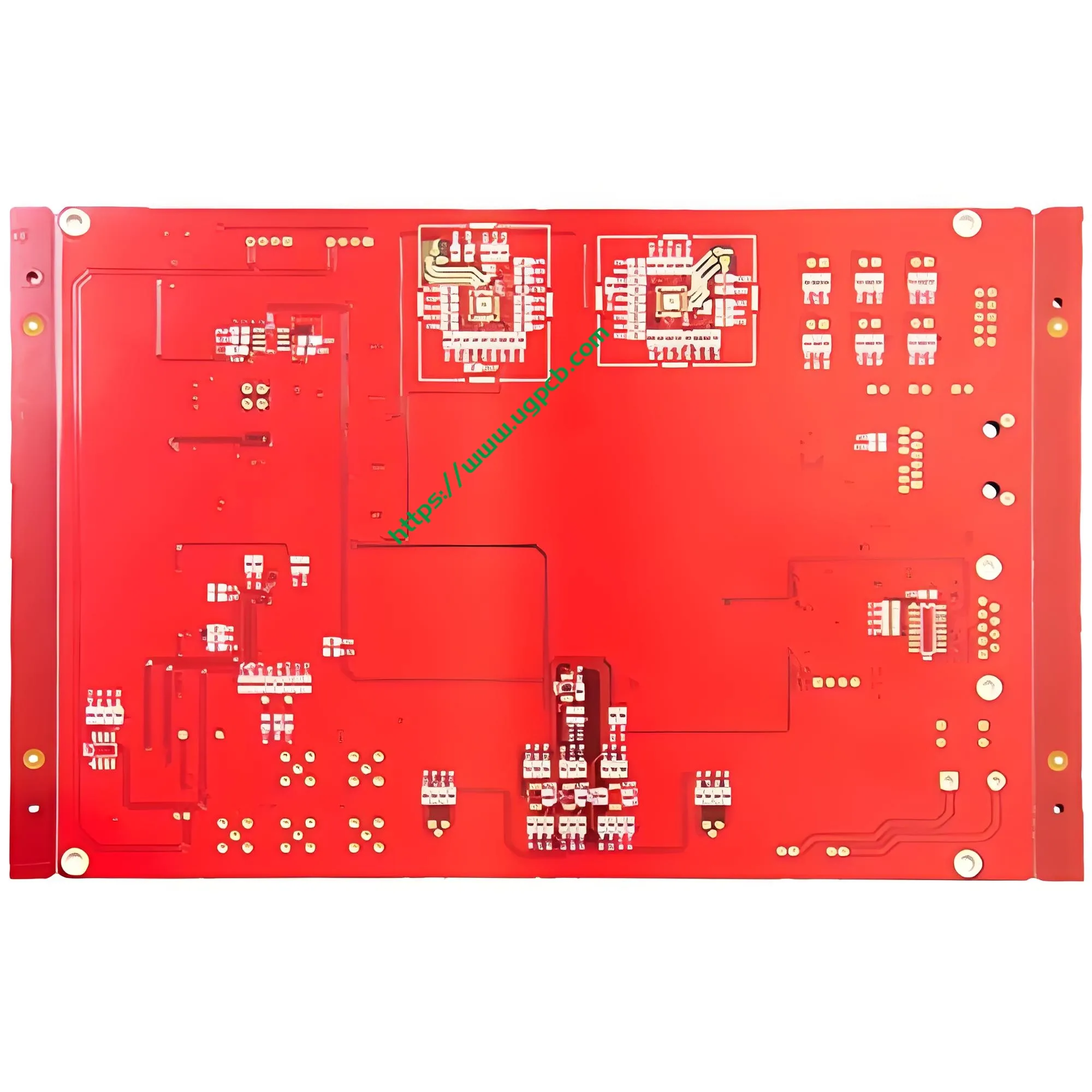
я. Обзор продукта: Прецизионная печатная плата, разработанная для эстетического оборудования
Инструмент для лазерной эпиляции основан на базовой системе управления.. Эта система диктует безопасность, стабильность, и общая эффективность лечения. В основе этой системы лежитпечатная плата прибора для лазерной эпиляции. Этот компонент совсем не тривиален.
УГКПБ представляетдвухслойная жесткая печатная плата именно для этой цели. Мы производим эту плиту с использованием высококачественного эпоксидного ламината, армированного стекловолокном FR4.. Толщина доски составляет 1,0 мм.. Его компактные размеры 53.68 х 37,5 мм. Мы специально адаптируем эти спецификации к ограничениям внутреннего пространства современных портативных и профессиональных лазерных устройств..
Этот печатная плата поддерживает оба IPL интенсивный импульсный свет и диодный лазер системы удаления волос. Это гарантирует стабильные электрические соединения и надежную передачу сигнала.. Превосходный печатная плата (Печатная плата в сборе) составляет основу высокопроизводительного эстетического оборудования. UGPCB специализируется на обеспечении высокой надежности, высокоточные печатные платы для мировых производителей косметических устройств.
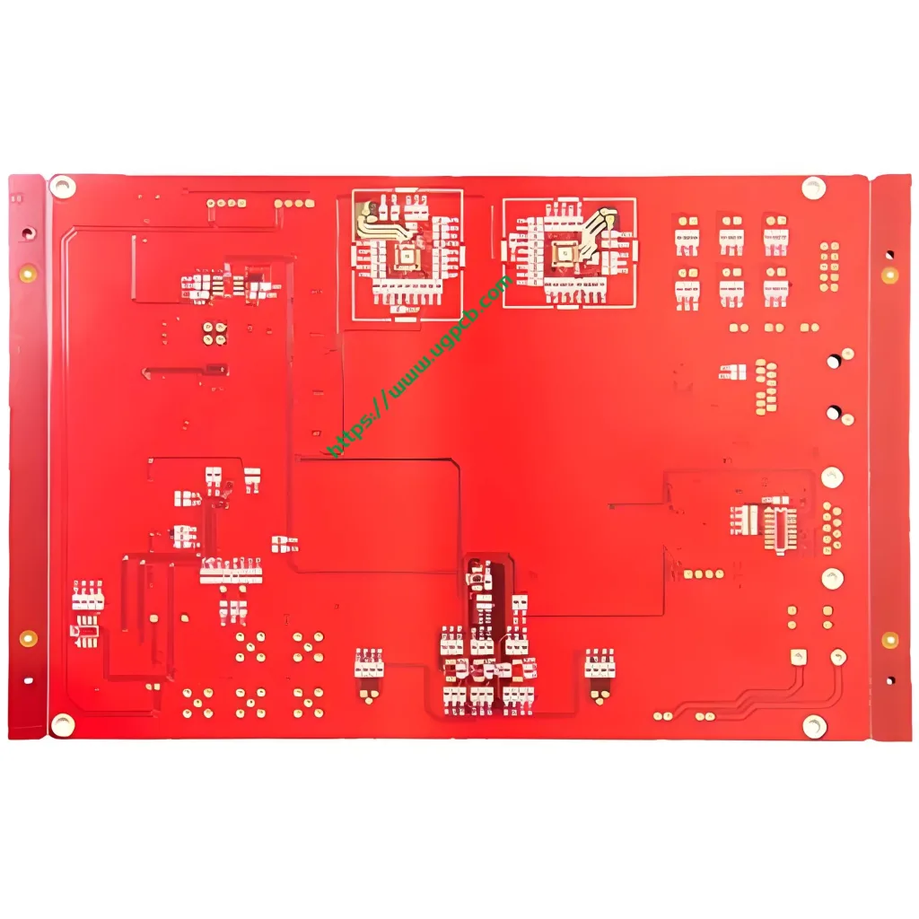
II. Определение продукта: Что такое печатная плата прибора для лазерной эпиляции??
Апечатная плата прибора для лазерной эпиляции это специальная печатная плата. Он управляет основными функциями, такими как распределение мощности., управление лазерным драйвером, мониторинг температуры, и взаимодействие с пользовательским интерфейсом.
Думайте об этом как о центральной нервной системе устройства.. Он точно передает электрическую энергию от батареи к лазерному генератору.. Он одновременно контролирует температуру системы, регулирует уровень энергии, и обрабатывает ввод кнопок.
Технически, этот продукт являетсядвусторонний, жесткая печатная плата со сквозными отверстиями. Он использует материал FR4.. Согласно МПК-6012 (Квалификационные и эксплуатационные характеристики жестких печатных плат), эта доска подходит для жесткого типа с металлическими отверстиями. Наш продукт соответствуетСорт 2 требования (Электронные продукты, предназначенные для специального обслуживания). Этот класс подходит для устройств, где высокая надежность важна, но не является критически важной., такие как системы удаления волос для домашнего и салонного использования..
III. Основы дизайна: Инженерная точность
Превосходный дизайн печатной платы выходит далеко за рамки простого подключения. Наша команда инженеров уделяет особое внимание нескольким критическим факторам для этой печатной платы для лазерной эпиляции..
3.1 Изоляция и защита от помех
Инструменты для лазерной эпиляции содержат как высоковольтные схемы управления, так и низковольтные схемы управления.. Электромагнитные помехи (Эми) между этими доменами часто вызывает нестабильность. UGPCB физически изолирует силовые и сигнальные контуры. Мы используем рациональное наложение слоев и оптимизированную маршрутизацию для эффективного уменьшения взаимных помех..
3.2 Компактная планировка и оптимизация пространства
The 53.68 Площадь основания x 37,5 мм требует интеграции высокой плотности. Наша команда дизайнеров обеспечивает комплексное размещение функциональных модулей в этом ограниченном пространстве.. Такая плотная прокладка обеспечивает превосходные электрические характеристики и позволяет миниатюризировать устройство..
3.3 Тепловое управление
Цепи лазерного драйвера выделяют значительное количество тепла во время работы.. Печатная плата действует как основной путь теплопроводности.. FR4 обладает собственной теплопроводностью.. В сочетании с оптимизированной заливкой меди и размещением термических переходов., наша конструкция эффективно рассеивает тепло. Такой подход повышает надежность устройства и продлевает срок его эксплуатации..
3.4 Соблюдение стандартов проектирования IPC
МПК-2221 (Общий стандарт проектирования печатных плат) рекомендует минимальный электрический зазор 0,1 мм. (4 мил) для общего оборудования. В нашем дизайне используется ширина линий и интервал0.36мм и 0,38 мм. Эта спецификация намного превышает минимальные требования. Это обеспечивает существенный запас прочности для электрических характеристик..
IV. Принцип работы: Как печатная плата управляет лазерным излучением
Принцип лазерной эпиляции прост., однако точное управление требует сложной координации печатной платы. Весь рабочий процесс следует этим шагам:
Шаг 1: Входная мощность и управление. Аккумулятор или адаптер обеспечивают чистую мощность.. Схема управления питанием печатной платы регулирует, фильтры, и распределяет эту энергию. Он обеспечивает чистую, стабильное напряжение на всех функциональных модулях.
Шаг 2: Контроль уровня энергии. Пользователь выбирает уровень энергии (обычно 5 регулируемые настройки). MCU (Микроконтроллер) на плате получает эту команду. Затем он отправляет ШИМ (Широтно-импульсная модуляция) сигнал. Этот сигнал точно управляет схемой драйвера лазера., регулировка выходного тока лазерного генератора.
Шаг 3: Лазерное вождение и излучение. Схема драйвера преобразует электрическую энергию в точный рабочий ток для лазерного диода.. Этот ток заставляет лазер излучать определенную длину волны. (обычно 808 нм или 1064 нм).
Шаг 4: Мониторинг и защита в реальном времени. Датчики температуры на печатной плате постоянно контролируют тепловое состояние устройства.. MCU автоматически снижает мощность или отключает выход, если температура превышает безопасные пороги.. Печатная плата также выполняет функции обнаружения контакта с кожей и подсчета выстрелов.. Вся эта сложная логика безупречно работает на 53.68 доска х 37,5 мм.
В. Основные приложения и сценарии использования
Мы проектируем этопечатная плата для лазерной эпиляции для разнообразных применений в эстетической индустрии.
| Поле приложения | Конкретный вариант использования | Типовое оборудование |
|---|---|---|
| Домашний уход за красотой | Персональная эпиляция | Устройства IPL для домашнего использования, домашние лазерные системы |
| Профессиональные салоны | Коммерческие эстетические услуги | Профессиональное диодное лазерное оборудование. |
| Медицинская эстетика | Клиническое лечение | Системы медицинской лазерной терапии |
| ODM/OEM производство | Контрактное производство | Фирменная плата устройства для депиляции в сборе |
Более того, логику проектирования и производственные процессы этой печатной платы можно адаптировать. Они подходят для других эстетических устройств, включаяаппараты для фотоомоложения, средства для удаления пигментации, и РФ (радиочастота) косметические инструменты.
VI. Классификация продуктов
Мы можем научно классифицировать этот продукт по нескольким параметрам.:
- По материалу подложки: Жесткая печатная плата из эпоксидной стеклоткани FR4
- По количеству слоев: 2-слой (стандартная двусторонняя жесткая доска)
- По отделке поверхности: СОГЛАШАТЬСЯ (Химическое никель, иммерсионное золото) / Процесс золотого покрытия
- По классу воспламеняемости: UL 94 В-0 огнестойкий сорт
- По приложению: Потребительская медицина / плата эстетического устройства
- По уровню производительности IPC-6012: Сорт 2 (Электронные продукты, предназначенные для специального обслуживания)
VII. Материальная композиция: Гарантия качества FR4
7.1 FR4 Ламинат с медным покрытием
Мы изготовляем эту печатную плату, используяFR4 стеклоэпоксидный ламинат с медным плакированием. FR4 является преобладающей подложкой в индустрии печатных плат.. Состоит из тканого стекловолокна, пропитанного эпоксидной смолой., отверждается под воздействием высокой температуры и давления. Для МПК-4101 (Спецификация базовых материалов для жестких и многослойных печатных плат), FR4 демонстрирует эти важные свойства:
- Температура стеклянного перехода (Тг): 130–140°С
- Диэлектрическая проницаемость (Дк): 4.3–4,8 @ 1 МГц
- Рейтинг воспламеняемости: Соответствует UL 94 В-0
- Коэффициент термического расширения (КТР): 12–18 частей на миллион/°C
Конкретно, согласно МПК-4101/21, стандартные платы FR-4 имеют Tg (метод ТМА) от 110°C до 135°C. UGPCB выбирает материалы, которые значительно превышают этот базовый уровень..
7.2 Медная фольга
УГКПБ применяется35/35мкм (1унция/1 унция) медная фольга с обеих сторон. Спецификация в 1 унцию представляет собой наиболее широко используемую толщину меди.. Он обеспечивает оптимальный баланс между допустимой нагрузкой по току и экономической эффективностью..
7.3 Паяльная маска и чернила Legend
Мы применяемкрасная паяльная маска (красное масло) в сочетании сбелые персонажи шелкографии (белый текст) . Эта высококонтрастная схема имеет ряд преимуществ.. Это облегчает автоматизированный оптический контроль. (АОИ). Это также облегчает ручную проверку., переделка, и обслуживание. Более того, маска защищает следы меди от окисления, шорты, и перемычка припоем во время сборки.
VIII. Технические параметры и соответствие стандартам
8.1 Сводка ключевых параметров
| Параметр | Спецификация | Примечания |
|---|---|---|
| Базовый материал | ФР4 | Эпоксидный стеклотканевый ламинат |
| Толщина доски | 1.0мм | Стандартная жесткая толщина |
| Количество слоев | 2 слои | Двусторонняя маршрутизация |
| Размеры | 53.68 х 37,5 мм | Компактный форм-фактор |
| Минимальная апертура | 0.33мм (приблизительно. 13 мил) | Возможность точного сверления |
| Ширина линии / Расстояние | 0.36мм / 0.38мм (14.2/15 мил) | Превышает требования к разрешению IPC-2221. |
| Медная толщина фольга | 35/35мкм (1унция/1 унция) | Двусторонняя тяжелая медь |
| Поверхностная отделка | СОГЛАШАТЬСЯ (Химическое никель, иммерсионное золото) | Процесс золотого покрытия |
| Спорная маска цвет | Красный | Красное масло |
| Цвет легенды | Белый | Белый текст |
8.2 Соответствие стандартам
Разработка и производство нашей продукции строго соответствуют этим международным стандартам.:
- МПК-6012: Квалификация и производительность жесткой печатной платы
- МПК-4101/21: Спецификация материала ламината FR-4
- МПК-А-600: Приемлемость печатных плат
- МПК-4552: Спецификация поверхности ENIG
- UL 94 В-0: Самый высокий класс воспламеняемости для пластиковых материалов.
8.3 Проверка надежности
Для МПК-6012, жесткие плиты должны пройти несколько тестов на соответствие качества. УГКПБ выполняет 100% электрические испытания (летающий зонд или специальное тестирование приспособлений) на каждой доске. Этот процесс обеспечивает безупречную электрическую целостность перед отправкой.. Наши доски последовательно проходят:
- Электрические испытания: Непрерывность, сопротивление изоляции, диэлектрическое выдерживаемое напряжение
- Механические испытания: Прочность на очистку, коробление, стабильность размеров
- Экологические испытания: Термический стресс, циклическое изменение температуры, устойчивость к влажности
IX. Конструктивные особенности и физические характеристики
9.1 Двухслойная конфигурация
Этот2-слой печатной платы имеет медную схему как на верхней, так и на нижней стороне подложки FR4.Покрытые сквозные отверстия (ПТХ) обеспечить электрическое соединение между слоями. Эта структура обеспечивает высокую плотность маршрутизации при одновременном контроле производственных затрат.. Это наиболее экономичный тип печатной платы для бытовой электроники..
9.2 Минимальная диафрагма 0,33 мм
Минимальная диафрагма 0,33 мм. (13 мил) демонстрирует УГКПБвозможность прецизионного сверления. IPC-6012 требует жесткого контроля допусков и достаточной толщины покрытия внутри стенки отверстия.. Наш процесс гарантирует постоянное соблюдение этих спецификаций., гарантия долговременной надежности металлизированных соединений.
9.3 Ширина линии/точность интервала (0.36/0.38мм)
Ширина дорожки 0,36 мм и зазор 0,38 мм обеспечивают существенный запас электробезопасности.. По сравнению с базовой линией IPC-2221 0,1 мм., наша конструкция уменьшает перекрестные помехи и устраняет риск короткого замыкания. Эта консервативная, но точная маршрутизация повышает целостность сигнала в шумных средах с высокой мощностью..
9.4 Преимущества отделки поверхности ENIG
Мы принимаемХимическое никель, иммерсионное золото (СОГЛАШАТЬСЯ) для обработки поверхности, полностью соответствует IPC-4552. Этот процесс золотого покрытия дает явные преимущества:
- Превосходная паяемость: Слой золота защищает никель от окисления., гарантируя отличное формирование паяного соединения.
- Плоская копланарность: ENIG обеспечивает исключительно гладкую поверхность., идеально подходит для сборки компонентов с мелким шагом.
- Увеличенный срок годности: Покрытие устойчиво к окислению, возможность длительного хранения без ухудшения производительности.
- Совместимость склеивания алюминиевой проволоки: Эта отделка соответствует особым требованиям к упаковке высокого класса..
IPC-4552 определяет толщину слоя никеля 3–6 мкм и минимальную толщину слоя золота 0,05 мкм.. Процесс ENIG UGPCB строго соответствует этим спецификациям..
Х. Схема производственного процесса
Производство высококачественной печатной платы для лазерной эпиляции требует строгого подхода., многоэтапный рабочий процесс. UGPCB следует этой точной последовательности.:
- Резка: Мы разрезаем большие панели FR4 с медным покрытием на куски удобного производственного размера..
- Бурение: Сверлильные станки с ЧПУ создать все сквозные отверстия, включая прецизионные апертуры 0,33 мм..
- Химическое осаждение меди & Панельное покрытие: Мы химически осаждаем тонкий слой меди внутри отверстий.. В результате этого процесса создается проводящий цилиндр ПТГ., включение межуровневого соединения.
- Перенос узора: Мы ламинируем, разоблачать, и создайте фоторезистную пленку для переноса рисунка схемы на медные поверхности..
- Офорт: Химическое травление удаляет ненужную медь., оставляя окончательный рисунок схемы с точной шириной дорожки 0,36 мм..
- Прикладная маска: Наносим красную краску для паяльной маски.. Это покрытие защищает схему и определяет открытые площадки для пайки..
- Поверхностная отделка (СОГЛАШАТЬСЯ): Наносим химический слой никеля и иммерсионного золота., полностью соответствует IPC-4552.
- Печать легенд: Печатаем белую шелкографическую легенду, четкая маркировка обозначений компонентов и индикаторов полярности.
- Электрические испытания: Мы выполняем 100% летающий зонд или электрические испытания на основе приспособлений для проверки производительности.
- Маршрутизация / V-резка: Фрезеруем или V-образно обрезаем производственную панель до окончательной 53.68 размер х 37,5 мм.
- Окончательный контроль качества & Упаковка: Мы проверяем платы по критериям IPC-A-600.. Принятые платы упаковываются в вакуумную упаковку для защиты во время транспортировки..
XI. Почему стоит выбрать UGPCB для печатной платы вашего устройства для лазерной эпиляции?
11.1 Авторитетное одобрение стандартов
UGPCB строго соответствует IPC-6012., МПК-4101, МПК-А-600, и стандарты IPC-4552. Каждый процесс, от выбора материала до окончательной проверки, следует проверяемым отраслевым стандартам. Наше качество выдерживает самые строгие проверки.
11.2 Передовое точное производство
Наша способность производить минимальную апертуру 0,33 мм и ширину линий/интервал 0,36/0,38 мм подчеркивает наш технический опыт.. Мы обладаем точностью, необходимой для сложных задач лазерной эпиляции..
11.3 Глубокий опыт в эстетической индустрии
UGPCB обладает обширными знаниями в области печатных плат для эстетических устройств.. Мы хорошо понимаем уникальные требования к лазерному оборудованию., IPL, и оборудование для фотоомоложения, включая высоковольтную изоляцию., тепловое управление, подавление электромагнитных помех, и строгие ограничения надежности.
11.4 UL 94 В-0 Обеспечение воспламеняемости
Мы используем материалы, соответствующиеUL 94 В-0 рейтинг — высшая классификация огнестойкости.. Согласно UL94, В-0 требует, чтобы каждый образец горел в течение ≤10 секунд после каждого воздействия пламени.. Общее время горения набора из пяти образцов должно составлять не более 50 секунд.. Более того, никакие горящие капли не могут воспламенить вату, находящуюся под ней.. Это обеспечивает максимальную безопасность, даже в ненормальных условиях эксплуатации.

XII. Свяжитесь с нами для получения индивидуального решения для печатной платы
УГКПБ обеспечивает высокое качествоПечатные платы для лазерной эпиляции и под ключпечатная плата услуги мировым производителям эстетических устройств. Мы ваш идеальный партнер, если вы:
- Инженер-конструктор, разрабатывающий системы удаления волос нового поколения..
- Менеджер по закупкам ищет надежного поставщика печатных плат..
- Менеджер по продукту, которому требуются индивидуальные решения PCBA.
- Предпринимательская команда выходит на рынок косметических устройств.
Свяжитесь с нами сегодня для получения технического описания продукта, конкурентное предложение, или бесплатная техническая консультация!
📧 Электронная почта: [info@ugpcb.com]
🌐 Сайт: [www.ugpcb.com]
📞 Телефон: [+86-135 4412 8719]
XIII. Заявление об источнике данных
Технические стандарты и данные о производительности, приведенные в этой статье, получены от следующих авторитетных учреждений.:
- МПК (Ассоциация, объединяющая электронную промышленность) — Указанные стандарты включают IPC-6012. (Квалификационные и эксплуатационные характеристики жестких печатных плат), МПК-4101 (Спецификация базовых материалов для жестких и многослойных печатных плат), МПК-А-600 (Приемлемость печатных плат), МПК-2221 (Общий стандарт проектирования печатных плат), и МПК-4552 (Спецификация для химического никеля/иммерсионного золота (СОГЛАШАТЬСЯ) Покрытие печатных плат).
- UL (Андеррайтеры лаборатории) — УЛ 94 (Стандарт на испытания на воспламеняемость пластмассовых материалов для деталей устройств и приборов) В-0 Рейтинг пламени.
- Отраслевые технические публикации — Параметры свойств материала FR4 (Тс 130–140°С, Дк 4,3–4,8 @ 1 МГц, КТР 12–18 частей на миллион/°C) являются признанными эталонными значениями из таблиц данных композитных материалов и рекомендаций IPC-4101..













