

1. Обзор продукта
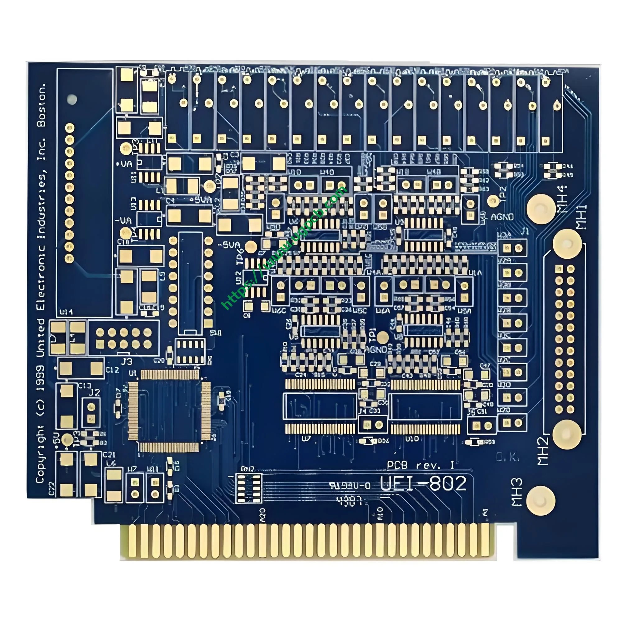
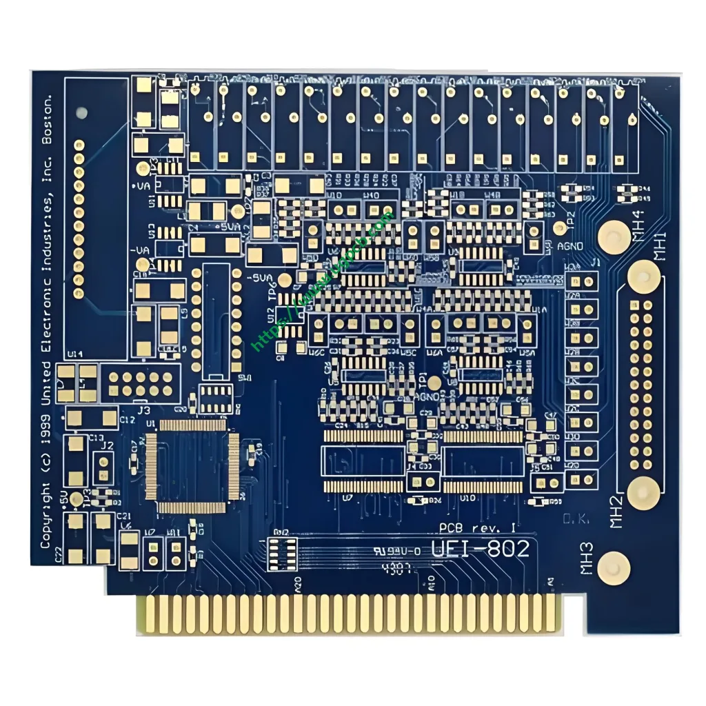
Двусторонний золотой палец печатная плата (печатная плата) имеет позолоченные контакты, обычно называемые «золотыми пальцами», расположенные вдоль края платы. Эти контакты создают подключаемый электрический путь при вставке в ответный разъем., например слот для карт или розетка. Все сигналы и мощность проходят через эти пальцеобразные клеммы..
В двусторонней печатной плате UGPCB с золотыми пальцами используется подложка FR4 с двухслойной конструкцией.. Толщина доски составляет 1.6 мм, и внутренний, и внешний слои имеют 1 Оз меди. Минимальный диаметр просверленного отверстия составляет 0.3 мм, и ширина трассы, и интервал оба 0.15 мм. Покрытие поверхности – иммерсионное золото. (СОГЛАШАТЬСЯ) по всей доске, с дополнительным гальваническим покрытием из твердого золота, выборочно нанесенным на участки золотых пальцев. Этот продукт обеспечивает гибкость разводки двусторонней платы и проверенную надежность соединений с золотыми пальцами.. Он обслуживает широкий спектр электронных систем, для которых требуются подключаемые интерфейсы «плата-плата»..
2. Классификация и позиционирование продукции
Согласно IPC‑6012 (квалификация и характеристики жесткой печатной платы), этот продукт попадает в следующие категории:
| Классификация Измерение | Категория |
|---|---|
| По структуре | Двусторонняя печатная плата – проводящие дорожки с обеих сторон |
| По методу соединения | Со сквозными металлизированными отверстиями (ПТХ) |
| По классу производительности IPC‑6012 | Сорт 2 (электронные продукты для специального обслуживания) – подходит для большинства применений с золотыми пальцами |
| По материалу подложки | Жесткий ламинат FR4 (Сорт S1141) |
| По отделке поверхности | СОГЛАШАТЬСЯ (химический никель / Погружение золота) + селективное гальваническое твердое золото на золотых пальцах |
| По функции | Печатная плата с золотым пальцем / крайний разъем печатной платы |
Этот продукт позиционируется какШтекерное соединение средней и высокой надежности решение. Он сочетает в себе свободу проектирования двусторонней разводки с целостностью сигнала разъемов с позолоченными краями..
3. Ключевые технические параметры
3.1 Субстрат: ФР4 + S1141 Ламинат
FR4 — наиболее распространенная жесткая подложка в индустрии печатных плат.. Состоит из эпоксидной смолы, армированной стекловолокном., что обеспечивает превосходную механическую прочность, электрическая изоляция, и термическое сопротивление. Этот продукт использует S1141 FR4 ламинат от Shengyi Technology, который соответствует IPC‑4101/21.
Ключевые показатели эффективности S1141 (протестировано на 1.6 мм образцы) перечислены ниже.
| Параметр | Типичное значение | Метод испытания |
|---|---|---|
| Температура стеклянного перехода (Тг) | 140°С (ДСК) | IPC‑TM‑650 2.4.25 |
| Температура термического разложения (Тд) | 310°С (5 % потеря веса) | IPC‑TM‑650 2.4.24.6 |
| CTE по оси Z (до Тг) | 65 ppm/° C. | IPC‑TM‑650 2.4.24 |
| CTE по оси Z (после Тг) | 300 ppm/° C. | IPC‑TM‑650 2.4.24 |
| Диэлектрическая проницаемость (Дк, 1 МГц) | 4.6 | IPC‑TM‑650 2.5.5.9 |
| Коэффициент рассеяния (Дф, 1 МГц) | 0.015 | IPC‑TM‑650 2.5.5.9 |
| Рейтинг воспламеняемости | UL 94 В‑0 | UL 94 |
| Водяной поглощение | 0.15 % | IPC‑TM‑650 2.6.2.1 |
Источник данных: Технический паспорт Shengyi S1141, соответствует IPC‑4101/21.
UL 94 В‑0 является самым высоким рейтингом огнестойкости в UL 94 испытание на вертикальное горение. Требуется, чтобы после двух 10-секундных воздействий пламени, общее время пламенного горения каждого образца не превышает 10 секунды, и никакие горящие капли не зажгут ватный индикатор. Это гарантирует, что печатная плата останется безопасной в условиях аномального нагрева или короткого замыкания..

3.2 Толщина доски: 1.6 мм
The 1.6 Толщина в мм является отраслевым стандартом для жестких печатных плат.. Она также служит базовой толщиной для данных о свойствах материала S1141.. Такая толщина обеспечивает оптимальный баланс между механической прочностью., стабильность вставки, и стоимость изготовления. Он широко совместим со стандартными разъемами разъемов..
3.3 Толщина меди: 1 унция (Примерно 35 мкм)
Медная фольга как внутреннего, так и внешнего слоя1 унция (унция) , что примерно 35 мкм толщиной. Согласно IPC‑6012, минимальная толщина готовой меди для класса 1 и класс 2 доски это 48 мкм. Начиная с 1 Фольга на унцию гарантирует, что окончательная толщина после обработки соответствует этим требованиям.. Этот медный груз поддерживает достаточную токовую нагрузку. (примерно 4‑6 А, в зависимости от ширины дорожки) сохраняя при этом точность травления тонких линий. Ширина трассы и расстояние между 0.15 мм (о 6 мил) надежно производятся с 1 Оз меди.
3.4 Минимальный диаметр отверстия: 0.3 мм
Минимальный диаметр механического отверстия составляет 0.3 мм, что вполне соответствует возможностям стандартной технологии сквозных отверстий. Это поддерживает металлизированное сквозное отверстие. (ПТХ) обработка для обеспечения надежного электрического соединения между слоями. Для IPC‑6012, все PTH должны пройти испытания на термическую нагрузку (288 °C погружение припоя) для проверки структурной целостности.
3.5 Ширина следа и расстояние: 0.15 мм / 0.15 мм
Ширина следа 0.15 мм (примерно 6 мил) и интервал 0.15 мм представляют собой тонкую линию в традиционном производстве печатных плат.. В 1 Оз. Толщина меди, а 0.15 След мм может выдерживать ток примерно 0,5–0,8 А согласно расчетам IPC-2221.. Это отвечает потребностям большинства приложений передачи сигналов и источников питания с низким энергопотреблением.. Такое сочетание ширины и расстояния обеспечивает надежность, сохраняя при этом производственные затраты под контролем..
4. Поверхностная отделка: Иммерсионное золото плюс гальванизированные золотые пальцы
В этом продукте используетсякомбинированный процесс отделки поверхности: Погружение золота (СОГЛАШАТЬСЯ) по всей доске, сгальваническое твердое золото выборочно наносится на участки золотых пальцев. Это стандартный и оптимальный процесс для печатных плат с золотыми пальцами..
4.1 Погружение Золото (СОГЛАШАТЬСЯ) Процесс
Химический никель / Погружение Золото (СОГЛАШАТЬСЯ) это отделка, при которой никель сначала химически осаждается на медную поверхность., за которым следует тонкий слой золота, нанесенный в результате реакции замещения.
ПерIPC‑4552 Редакция А (изданный 2017) :
- Толщина никеля: 3 мкм до 6 мкм (120 мкин до 240 мин)
- Толщина золота: 0.04 мкм до 0.10 мкм (1.6 мкин до 4.0 мин)
- Рекомендуемая толщина золота: 0.04 мкм до 0.07 мкм (1.6 мкин до 2.8 мин)
Источник данных: IPC‑4552 – Технические характеристики химического никеля / Погружение Золото (СОГЛАШАТЬСЯ) Покрытие печатных плат.
Преимущества ЭНИГ:
- Плоская поверхность подходит для дорожек с мелким шагом и корпусов BGA.
- Отличная паяемость, поддерживающая бессвинцовую пайку. (например, SAC305)
- Сильная стойкость к окислению и длительный срок хранения.
- Тонкий слой золота позволяет контролировать затраты
4.2 Золотые пальцы с гальваническим покрытием – ключевая особенность
Области золотых пальцев получаютдополнительное гальваническое твердое золото. В отличие от мягкого золота, используемого в ENIG, гальваническое твердое золото содержит отвердители, такие как кобальт или никель (золото-кобальтовый или золото-никелевый сплав). Его твердость может превышать HV. 200, обеспечивая гораздо большую износостойкость, чем мягкое золото.
Почему для золотых пальцев необходимо использовать гальваническое твердое золото??
Золото ENIG очень тонкое (всего 0,04‑0,10 мкм) и мягкий (твердость ниже HV 90). Он изнашивается всего за 3–5 циклов установки.. Гальваническое твердое золото, толщиной обычно выше 0.76 мкм, выдерживает сотни и даже тысячи циклов вставки.
ПерМПК‑4556 (Технические характеристики твердого золота) :
| Класс приложения | Минимальная толщина золота | Типичные приложения |
|---|---|---|
| Сорт 2 (Прочный) | ≥ 0.76 мкм (30 мин) | Большинство приложений с золотыми пальцами |
| Сорт 3 (Высокая надежность) | ≥ 1.27 мкм (50 мин) | Многоцикловая установка, промышленное / военный |
| Никелевая подложка | 3-5 мкм | Требуется для всех месторождений твердого золота. |
Источник данных: IPC‑4556 – Технические характеристики гальванического твердого золота для разъемов и золотых пальцев.
Технология нанесения гальванического покрытия золотыми пальцами, используемая в этом продукте, соответствует классу IPC-4556. 2 через класс 3 стандарты, обеспечение срока службы и надежности контакта.
5. Соображения дизайна
5.1 Снятие фаски с золотым пальцем
Вставной конец золотых пальцев должен бытьскошенный для обеспечения плавного входа в разъем разъема.
- Угол фаски: Обычно 30° или 45°.
- Глубина фаски: Для 1.6 мм толщина доски, глубина фаски обычно составляет 0,8‑1,0 мм., оставляя на кончике тупой край 0,6‑0,8 мм.
- Остаточная толщина наконечника: Примерно от одной трети до половины исходной толщины доски.
- Критическое требование: Никакая паяльная маска не должна закрывать скошенную область., и слой золота должен полностью покрывать скошенный скос
5.2 Правила проектирования зоны золотого пальца
- Золотые пальцы должны быть расположены на краю доски в упорядоченном порядке.
- Минимальное расстояние между соседними золотыми пальцами должно быть ≥ 7 мил (примерно 0.178 мм)
- Область золотого пальца должна быть четко обозначена в файлах Gerber с четкими инструкциями по нанесению покрытия.
5.3 Рекомендации по управлению импедансом
Материал FR4 имеет диэлектрическую проницаемость Dk = 4.6 в 1 МГц. Для 50 Ом несимметричный или 100 Управление дифференциальным импедансом Ом, дизайнеры могут регулировать ширину дорожки и толщину диэлектрика. The 0.15 Ширина и расстояние между дорожками в мм в этом изделии соответствуют большинству требований к целостности сигнала для стандартных конструкций..
6. Принцип работы
Двусторонняя печатная плата с золотыми пальцами работает посредством двух основных механизмов.: электрический контакт ипередача сигнала.
- Электрическое подключение: Позолоченные контакты на краю платы физически сопрягаются с металлическими пружинными контактами внутри разъема., создание электрического пути с низким сопротивлением.
- Передача сигнала: Печатная плата отслеживает сигналы маршрутов от различных компоненты (чипсы, резисторы, конденсаторы, и т. д.) к контактам золотых пальцев, которые затем передают через разъем на материнскую плату или объединительную плату.. Двусторонняя конструкция позволяет прокладывать как верхний, так и нижний слои, значительное увеличение плотности маршрутизации и гибкости конструкции.
- Возможность подключения: Гальванический слой твердого золота на золотых пальцах обеспечивает достаточную износостойкость, чтобы выдерживать несколько циклов вставки без ухудшения контактного сопротивления или целостности сигнала..
7. Приложения и варианты использования
Двусторонние печатные платы с золотыми пальцами широко используются в электронных устройствах, требующихсъемные соединения. Общие приложения включают в себя:
| Область применения | Конкретные продукты |
|---|---|
| Вычисление & Серверы | Модули памяти (Ддр, DDR2, DDR3, DDR4, Др5), видеокарты, сетевые карты, карты расширения |
| Бытовая электроника | USB-накопители, карты памяти, картридеры, смартфоны, умные часы |
| Коммуникационное оборудование | Маршрутизаторы, переключатели, модули связи |
| Промышленный контроль | Промышленные щиты управления, карты сбора данных, испытательные приспособления |
| Автомобильная электроника | Блоки управления автомобилем, информационно -развлекательные системы |
| Медицинские устройства | Медицинские электронные модули (с медицинской добавкой IPC‑6012EM) |
| Аэрокосмическая промышленность | Модули авионики (с аэрокосмическим дополнением IPC‑6012FS) |
Двусторонние печатные платы FR4 с золотыми пальцами особенно подходят длясредней сложности, чувствительные к затратам приложения которые требуют подключения к плагину.
8. Схема производственного процесса
UGPCB следует стандартной производственной последовательности для двусторонних печатных плат с золотыми пальцами.:
- Резка – Отрежьте медный ламинат FR4 по размерам рабочей панели..
- Бурение - Сверлить 0.3 мм сквозные и монтажные отверстия.
- ПТХ / Панельное покрытие – Применить химическое осаждение меди в отверстиях., затем панельная пластина.
- Перенос узора – Раскрыть и разработать схему схемы.
- Узорное покрытие – Электролитически пластинчатые цепи и отверстия для 1 Оз меди.
- Офорт – Удалите незащищенную медную фольгу, чтобы сформировать конечные дорожки цепи..
- Припаяя маска – Нанесите зеленые или другие цветные чернила для паяльной маски..
- Поверхностная обработка – ЭНИГ – Нанесите химический никель и иммерсионное золото по всей плате..
- Золотое покрытие пальцев – Выборочная гальваника твердого золота на участках золотых пальцев..
- Снятие фаски с золотым пальцем – Снять фаску на вставляемом конце.
- Электрические испытания - Выполнять летающий зонд или тестирование приспособлений.
- Визуальный осмотр – Проверьте согласно IPC‑A‑600..
- Упаковка & Перевозки — Вакуумная упаковка для защиты от влаги.
9. Стандарты производительности и качества
Этот продукт разработан и изготовлен в строгом соответствии со следующими международными стандартами.:
| Стандартный | Заголовок | Объем |
|---|---|---|
| МПК‑6012 | Квалификационные и эксплуатационные характеристики жестких печатных плат | Общая производительность и надежность |
| IPC‑A‑600 | Приемлемость печатных плат | Внешний вид и критерии приемки |
| МПК‑4552 | Технические характеристики ENIG | Управление процессом иммерсионного золота |
| МПК‑4556 | Технические характеристики гальванического твердого золота | Процесс твердого золота с золотым пальцем |
| МПК‑4101/21 | Спецификация на материалы подложки для жестких и многослойных печатных плат | Характеристики материала FR4 |
| UL 94 В‑0 | Стандарт безопасности – воспламеняемость пластиковых материалов | Сертификация огнестойкости |
10. Почему выбирают UGPCB?
- Профессиональный опыт производства золотых пальцев – UGPCB обладает развитыми возможностями в области гальваники и снятия фасок..
- Сквозной контроль качества – Каждый шаг от резки до окончательной проверки контролируется в соответствии со стандартами IPC..
- Прослеживаемые материалы – Используются фирменные ламинаты FR4, такие как Shengyi S1141, с четкой отслеживаемостью источника..
- Быстрая доставка – Специальная линия по производству двусторонних печатных плат обеспечивает быстрое прототипирование и серийное производство..
- Техническая поддержка – Обеспечивает DFM (Дизайн для производства) обзоры и рекомендации по контролю импеданса.
11. Запросить сейчас
UGPCB стремится поставлять высококачественные двусторонние печатные платы с золотыми пальцами клиентам по всему миру.. Нужен ли вамобразец прототипирования, мелкосерийное пробное производство, или крупносерийное производство, у нас есть опыт, чтобы служить вам.
Свяжитесь с нами для получения предложения:
- Предоставьте файлы Gerber или дизайн печатной платы данные
- Укажите толщину золотого покрытия (0.76 мкм до 1.27 рекомендуется мкм)
- Подтвердить угол фаски (30° или 45°) и любые другие особые требования
Декларация источника данных
Технические данные и ссылки на стандарты в этом документе взяты из: Квалификация и технические характеристики IPC‑6012 для жестких печатных плат; IPC‑4552 Технические характеристики для химического никеля / Погружение Золото (СОГЛАШАТЬСЯ) Покрытие печатных плат; Технические характеристики IPC‑4556 для гальванического твердого золота для разъемов и золотых пальцев; IPC‑A‑600 Приемлемость печатных плат; UL 94 Стандарт безопасности – воспламеняемость пластиковых материалов; и технический паспорт Shengyi S1141. (соответствует IPC‑4101/21).













