
Профессиональное определение: Что такое 6-слойная высокочастотная гибридная печатная плата?
В сфере связи 5G, Автомобильный радар, и высокопроизводительные компьютеры, стандартный Печатные платы FR-4 часто не удовлетворяют требованиям к высокочастотным, высокоскоростной, и высокая стабильность передачи сигнала. Именно здесь Высокочастотный Гибридная печатная плата становится критическим.
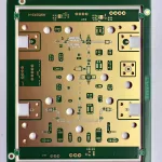
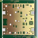
6-слойная высокочастотная гибридная печатная плата представляет собой многослойную печатную плату, объединяющую различные уровни производительности. высокочастотный ламинат материалы (такие как Роджерс) из стандартных или специализированных материалов посредством прецизионного ламинирования. Этот гибридная конструкция стратегически размещает материалы для оптимизации электрических, тепло, и экономичность на разных уровнях схемы. Он служит основная аппаратная основа для сложных РЧ СВЧ схемы и высокоскоростные цифровые проекты.

Глубокое знакомство с продуктом: Высокопроизводительная 6-слойная гибридная плата UGPCB
1. Основные спецификации & Материальная наука
-
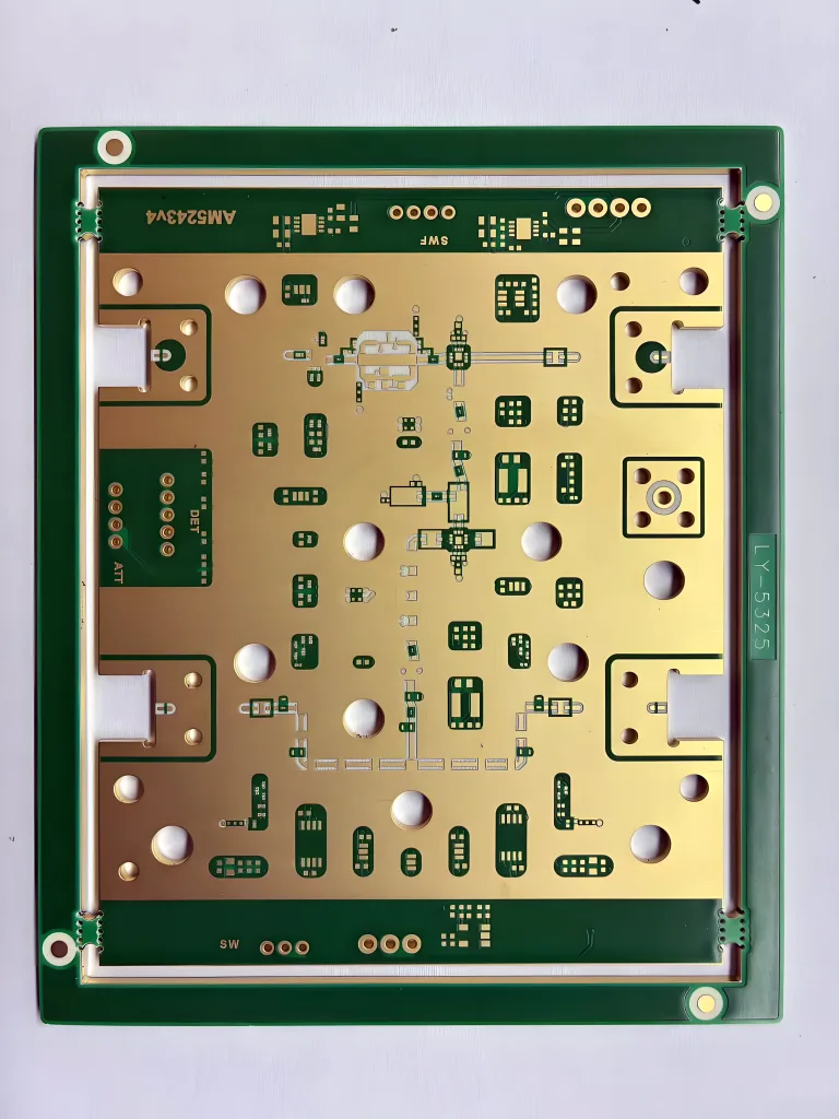
Слой & Строительство: 6 Слои. Это представляет собой оптимальный баланс между сложностью, производительность, и стоимость, подходит для интеграции цифрового управления и входных радиочастотных схем.
-
Укладка материалов (Гибридное ядро):
Rogers 4350B + Rogers 4450F + IT180A. В этом суть дизайна.-
Роджерс 4350b: Отраслевой стандарт материал высокочастотной печатной платы известен своей стабильной Диэлектрическая проницаемость (Дк) и низкий Коэффициент рассеяния (Дф), что делает его идеальным для слоев радиочастотного сигнала.
-
Роджерс 4450F: Препрег (ПП) с высокой температурой стеклования (Тг) и превосходная термическая стабильность, используется для склеивания слоев и обеспечения надежности гибридной сборки при термических нагрузках.
-
ИТ180А: Высокопроизводительный, Термореактивный материал со средними потерями, часто используемый для внутренних слоев сигнальной или силовой плоскости, где требуется хорошая целостность сигнала при разумных затратах.. Этот гибридный подход применяет лучший материал там, где он больше всего необходим..
-
-
Толщина & Медный вес: Стандартный 1.6мм толщина для хорошей механической жесткости. Вес меди
1/H/H/H/H/1 oz, указывая 1 медная фольга на унцию для внешних слоев и 0.5 унция (Г унций) медь для внутренних слоев. Это облегчает травление точных линий и оптимизирует контроль импеданса.. -
Поверхностная отделка: Электролетное никелевое электролетное погружение палладий Золото (Enepic): 120 Мне, 2 мкин Pd, 2 микроин Au. Это покрытие премиум-класса, обеспечивающее отличную паяемость., возможность проводного соединения, и коррозионная стойкость. Он особенно подходит для Подложки ИС и сборки, требующие нескольких циклов оплавления или соединения золотой проволокой..
2. Соображения дизайна & Принцип работы
-
Соображения дизайна:
-
Контроль импеданса & Целостность сигнала: Использование стабильных материалов Dk Роджерса., в сочетании с точной конструкцией стопки и контролем ширины и расстояния между дорожками, позволяет плотно Контроль импеданса печатной платы (например, 50Ом несимметричный, 100Ом дифференциал), что имеет решающее значение для целостность сигнала высокоскоростной печатной платы.
-
Планирование стека: Трассы высокоскоростных радиочастот обычно прокладываются по слоям материала Rogers., в то время как власть, земля, и низкочастотные цифровые сигналы размещаются на слоях IT180A.. Симметричный стек (как в этом дизайне) помогает предотвратить коробление.
-
Тепловое управление: Превосходная теплопроводность материалов Rogers, в сочетании со стратегическими наземными отверстиями и конструкциями терморазгрузки, способствует отводу тепла от мощных радиочастотных компонентов.
-
-
Принцип работы: Эта печатная плата действует как “скелет” и “система шоссейных дорог” электронного устройства. Его основная функция — монтировать и соединять компоненты. (RF чипы, процессоры, конденсаторы, и т. д.). Высокочастотные сигналы проходят через микроволновая печатная плата линии передачи на слоях Роджерса с минимальными потерями и искажениями; мощность распределяется стабильно через медные пластины внутреннего слоя; и сложные взаимосвязи достигаются за счет слепые и скрытые переходные отверстия, сокращение путей и улучшение электрических характеристик.
3. Четыре продвинутых процесса: Обеспечение надежности & Производительность
-
Основные слепые/скрытые переходные отверстия: Эти переходные отверстия соединяют соседние слои внутри ядра. (например, Роджерс ламинат) не проникая во всю доску. Это значительно увеличивает плотность маршрутизации в Взаимодействие высокой плотности (ИЧР) печатные платы, уменьшает паразитарные эффекты, и улучшает высокочастотные характеристики.
-
Заполненные смолой переходные отверстия: После покрытия, сквозные или глухие/скрытые переходные отверстия залиты эпоксидной смолой. Это предотвращает попадание химических веществ, обеспечивает ровную поверхность для нанесения мелкого рисунка на последующие слои, и улучшается за счет надежности.
-
Via-in-Pad (VIP): Переходное отверстие размещается непосредственно внутри контактной площадки компонента., затем заполняется и выравнивается смолой и медью. Это отличительная черта передовой HDI PCBS, обеспечивая дальнейшую миниатюризацию и более высокую плотность компонентов.
-
Металлизированный край (Покрытие края): Сплошной металлический слой (обычно медь) наносится по краю платы. Это обеспечивает превосходное Экранирование электромагнитных помех, защищает внутренние цепи, и укрепляет край для предотвращения спаривания разъема и механического износа.
4. Ключевые характеристики производительности
-
Превосходные высокочастотные характеристики: Низкая потеря, стабильный Dk для безупречной передачи сигнала в RF PCB.
-
Отличная целостность сигнала: Прецизионный контроль импеданса соответствует Высокоскоростной дизайн печатной платы требования.
-
Взаимодействие высокой плотности (ИЧР): Слепые/скрытые переходные отверстия и поддержка VIP-технологий Высокая печатная плата макеты.
-
Повышенная надежность: Прочная гибридная конструкция, ЭНЕПИГ отделка, и металлизированные края подходят для требовательных условий эксплуатации.
-
Улучшенный тепловой & Экранирующие характеристики: Хорошая теплопроводность и эффективное подавление электромагнитных помех..
5. Научная классификация
-
По количеству слоев: Многослойная печатная плата
-
По типу материала: Гибридный / Печатная плата из смешанного материала
-
По технологиям: Усовершенствованная печатная плата HDI
-
По приложению: РЧ-микроволновая печатная плата / Высокоскоростная цифровая печатная плата
6. Стандартный производственный процесс
Инженерное проектирование → Подготовка материалов & Стрижка → Лазерное сверление материалов Rogers (Слепые исчезновения) → Десмир & Металлизация → Визуализация внутреннего слоя & Офорт → Основное ламинирование (Гибридное соединение) → Механическое бурение → Смола начинка & Лечение → Визуализация внешнего слоя → ENEPIG Поверхностная обработка → Металлизированное покрытие кромок → Паяльная маска & Шелкография → Электрические испытания & Заключительная проверка.
7. Основные приложения (Варианты использования)
Этот продукт идеально подходит для высоконадежные электронные проекты с жесткими требованиями:
-
5G Коммуникационная инфраструктура: RF PCB внутри ЕУК (Активные антенные блоки) и удаленные радиоблоки.
-
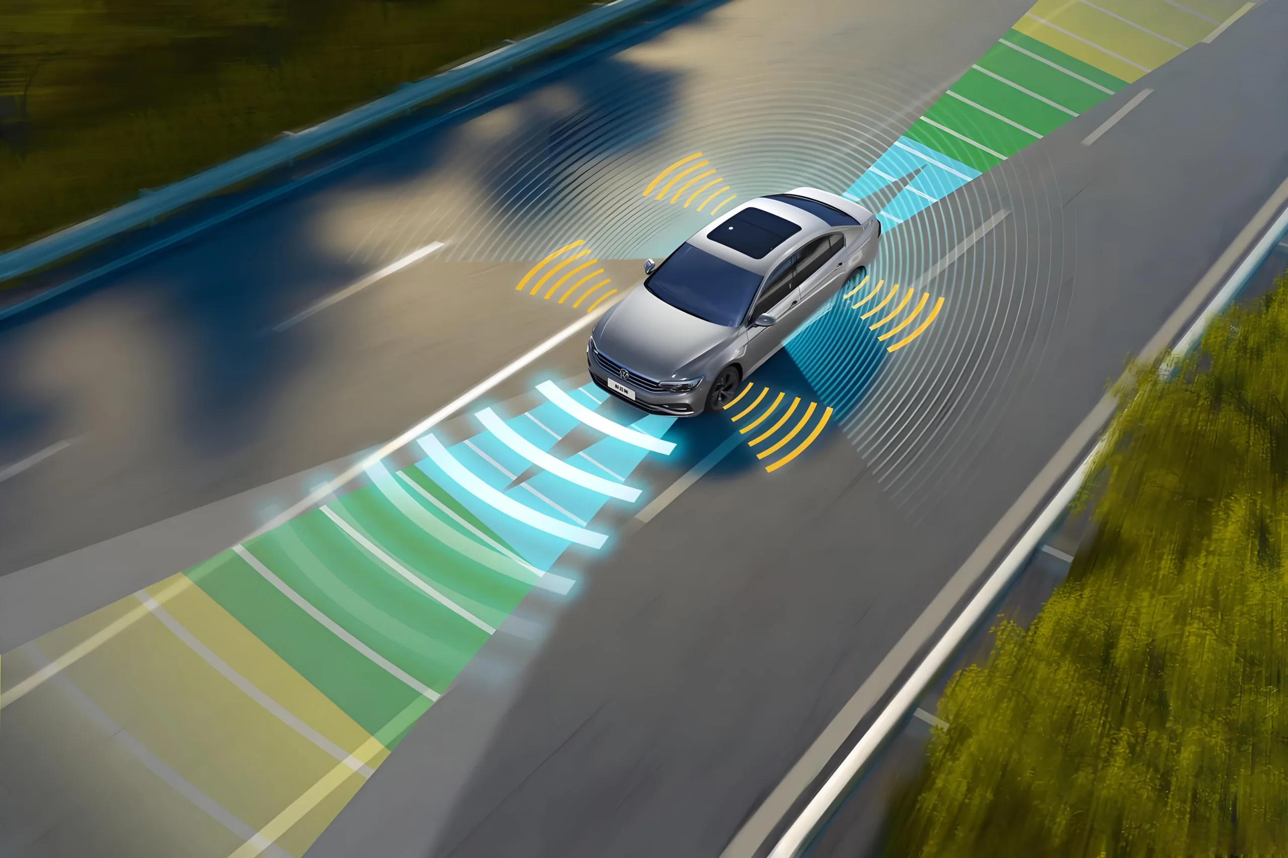
Автомобильная электроника: Радарные платы для ADAS и автономных транспортных средств (например, 77ГГц радар).
-
Аэрокосмическая промышленность & Оборона: Печатные платы высокой надежности в радиолокационных системах, спутниковая связь, и средства РЭБ.
-
Высококлассный тест & Измерение: Основные платы для анализаторов цепей и анализаторов спектра.
-
Высокопроизводительные вычисления & Центры обработки данных: Объединительные платы или материнские платы для высокоскоростных серверов/коммутаторов.
Почему стоит выбрать UGPCB для вашей 6-слойной высокочастотной гибридной печатной платы?
В продвинутом режиме Производство печатных плат, последовательность и внимание к деталям определяют успех. УГКПБ обладает глубоким опытом во всей сложной технологической цепочке — от Роджерс обработка материалов и лазерное бурение к смоляная начинка и ЭНЕПИГ покрытие. Мы поставляем не просто платы, соответствующие спецификациям, но крепкий Решения для печатных плат которые обеспечивают успешное массовое производство вашего продукта.
Свяжитесь с нами сегодня за специализированную техническую поддержку и конкурентоспособное предложение для вашего 5Г печатная плата, печатная плата автомобильного радара, или плата высокочастотного модуля проект. Пусть UGPCB станет вашим надежным партнером высокочастотный, высокоскоростное изготовление печатных плат.


