
SiP-подложка: Основная технология миниатюрной электроники
В сегодняшней быстро развивающейся электронике индустрии, smartphones are becoming slimmer yet more powerful, and wearable devices can accurately monitor various physiological metrics. Behind these breakthroughs lies a miniaturization revolution in electronic manufacturing, driven by System-in-Package (Глоток) технология. As the critical enabler of this revolution, the SiP packaging substrate plays an indispensable role in achieving high performance, high integration, и миниатюризация в электронных продуктах.
What is System-in-Package (Глоток) and the SiP Substrate?
Система-в-упаковки (Глоток) is an advanced electronic packaging technology that integrates multiple chips with different functions, пассивные компоненты, and other electronic elements into a single package, forming a complete system or subsystem.
Compared to traditional System-on-Chip (SoC), SiP offers greater design flexibility. A fitting analogy in the industry is: SoC is like a “fixed menu,” while SiP is a “buffet.” It allows engineers to freely select and combine different chips and components based on specific product functionality and performance requirements. This flexibility results in shorter product development cycles and relatively controllable costs, making it particularly suitable for consumer electronics with strict time-to-market demands.
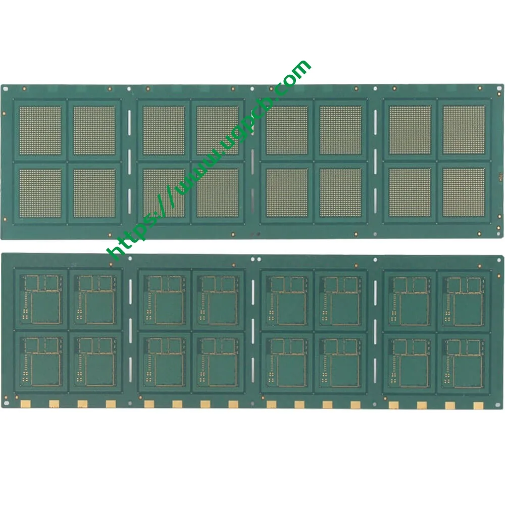
The SiP packaging substrate is the “тарелка” that carries this “buffet.” It is a special печатная плата manufactured using high-density interconnect (ИЧР) технология. It provides mechanical support, electrical connections, передача сигнала, and thermal pathways for the internal chips and components. Compared to standard PCBs, SiP substrates have extremely high requirements for line precision, interlayer connection density, and material performance, representing the pinnacle of Производство печатных плат технология.
UGPCB’s Premium SiP Packaging Substrate: Engineered for Precision Integration
To meet the market’s urgent need for high-integration SiP solutions, УГКПБ leverages its deep technical expertise in the PCB industry to offer a high-performance SiP packaging substrate. This product is specifically designed for complex IC packaging, aiming to provide customers with stable and reliable miniaturized interconnect solutions.
Основные технические характеристики:
| Параметр | Detailed Specification | Technical Advantage & Significance |
|---|---|---|
| Название продукта | SiP Packaging Substrate | Designed for System-in-Package, enabling high-density multi-chip integration. |
| Key Material | Shengyi Technology SI10U | Low-loss, high-reliability laminate ensuring signal integrity for high-frequency/high-speed signals. |
| Количество слоев | 6 Слои | Provides ample routing space; optimized power & ground plane design to reduce EMI. |
| Готовая толщина | 0.5 – 0.6 мм | Extremely thin, meeting stringent thickness requirements for wearables, phone modules, и т. д.. |
| Размеры | 35 х 35 мм | Compact layout, maximizing utilization of package space. |
| Припаяя маска | PSR-4000 AUS308 | High-precision, high-heat resistance solder mask ink protecting fine circuit lines. |
| Поверхностная отделка | Enepic (Электролетное никелевое электролетное погружение палладий Золото) | Excellent solder joint reliability and wire bonding capability. |
| Минимальный размер отверстия | 0.075мм (Micro via) / 0.1мм | Utilizes microvia technology to achieve ultra-high-density interlayer connections. |
| Мин. Ширина линии/пространство | 50мкм / 30мкм | Matches advanced HDI capabilities, supporting fine-pitch BGA/CSP chip connections. |
| Core Application | SiP Packaging IC Substrate | Suitable for RF front-end, sensor modules, power management units (PMUs), и т. д.. |
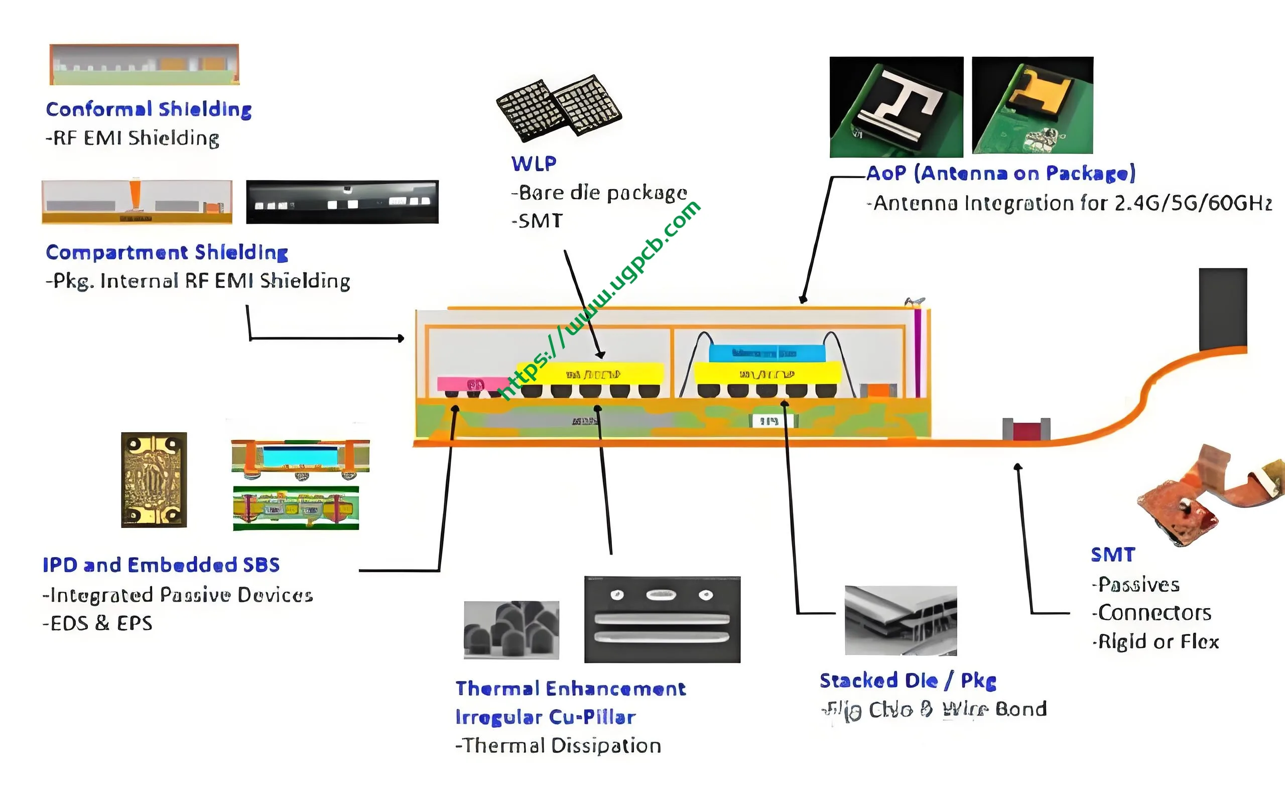
Our substrate features a 6-layer stack-up (typical structure: SIG/GND/PWR/SIG/GND/SIG). The dedicated power and ground planes not only manage power distribution effectively but also significantly reduce electromagnetic interference (Эми) between signals, enhancing system stability in complex environments. This design is particularly suitable for mixed-signal systems where high-speed digital and sensitive analog signals coexist.
Advanced Manufacturing Process for SiP Packaging Substrates
The manufacturing of SiP substrates is one of the most complex areas in PCB technology, extensively employing High-Density Interconnect (ИЧР) and build-up processes.
-
Core Process – Laser Drilling & Electroplating Fill: The product’s core is its dense microvias. We use high-precision laser equipment to drill micro-blind vias as small as 0.075mm in diameter. Впоследствии, advanced pulse electroplating fill technology ensures void-free copper deposition within these microvias. This technology handles microvias with an aspect ratio of up to 1.5:1, guaranteeing absolute reliability in interlayer electrical connections and providing low-impedance paths for signal transmission.
-
High-Precision Pattern Transfer: Utilizing a Modified Semi-Additive Process (Мсап) combined with ultra-precise exposure technology, the circuit design is transferred onto the copper foil. This enables us to consistently achieve 50μm fine lines, laying the foundation for a higher signal routing density per unit area (offering over 300% improvement compared to conventional processes).
-
Multi-Layer Lamination & Поверхностная отделка: Multiple core layers with precision circuits and prepreg are aligned accurately and laminated in a single press cycle. Окончательно, the ENEPIG surface finish is applied, depositing successive layers of nickel, palladium, and gold on the pads. This process combines the good solderability of ENIG (Химическое никель, иммерсионное золото) with the corrosion resistance and prevention of “черный коврик” issues provided by the palladium layer, offering a perfect surface for subsequent chip mounting and wire bonding.
Broad Application Scenarios: Powering Future Smart Devices
Thanks to their miniaturization, высокая производительность, и высокая надежность, UGPCB’s SiP packaging substrates have become the preferred solution in several cutting-edge technology fields:
-
-
Бытовая электроника & Коммуникации: В смартфонах, they integrate RF front-ends, Bluetooth/Wi-Fi modules, power management chips, и т. д., into a single module, enabling up to 57% reduction in overall module size and freeing up valuable space for batteries. They are also widely used in 5G communication modules and true wireless stereo (TWS) earbuds, enabling perfect integration of complex functions within confined spaces.
-
Автомобильная электроника: With the trend towards vehicle intelligence and electrification, the reliability requirements for electronic systems are extremely high. Our substrates can be used in Advanced Driver-Assistance Systems (Адас) sensor modules, in-vehicle infotainment system core units, и т. д., meeting the automotive-grade demands for high-temperature and high-vibration operating environments.
-
Высокопроизводительные вычисления & Ай: In AI accelerator cards and data center switch chip packaging, SiP substrates are responsible for high-speed SerDes signal transmission and low-latency interconnects between chips. Their excellent signal integrity is key to maintaining computing power.
- Интернет вещей & Носимые устройства: For devices like smartwatches and health monitoring patches, our ultra-thin, miniaturized substrates enable the integrated packaging of sensors, микропроцессоры, and wireless communication chips, achieving an extremely slim and light form factor and long battery life.
-

Choose UGPCB for Reliable, One-Stop PCB Solutions
UGPCB not only provides top-tier SiP packaging substrates but is also committed to offering customers a comprehensive one-stop electronic interconnect solution—from design support to volume production. Our services encompass дизайн печатной платы поддерживать, multi-type circuit board manufacturing, SMT Assembly, и full turnkey PCBA услуги. Our modern production facilities comply with a series of international certifications, including the IATF 16949 automotive quality management system, ensuring every product delivered to our customers possesses superior and consistent quality.
In the pursuit of ultimate performance and compact form factors in electronics today, a precision SiP packaging substrate could be the key to your product’s breakthrough. If you are seeking high-density, high-reliability packaging substrate or печатная плата решения, UGPCB’s professional team is ready to provide you with comprehensive support—from technical consultation to manufacturing.
Свяжитесь с нами сегодня, and let’s collaborate to condense your innovative ideas into a compact, powerful reality.


