

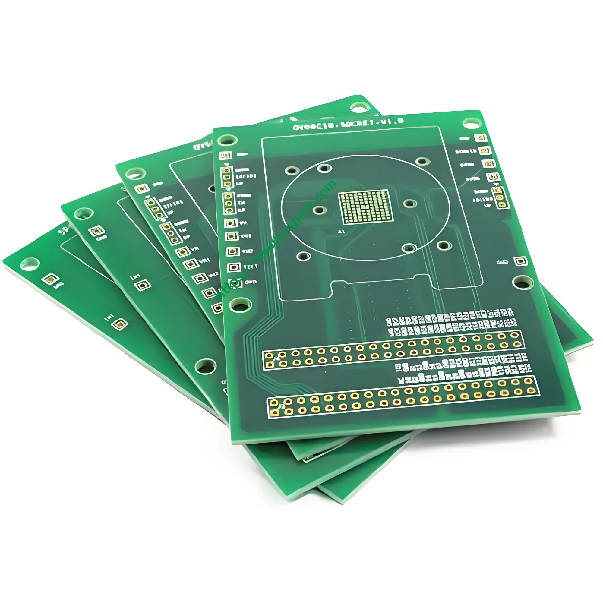
1. Обзор продукта: Что такое печатная плата беспроводного пылесоса?
Плата беспроводного пылесоса (Печатная плата) является основным электронным компонентом, отвечающим за управление приводом двигателя., управление питанием, взаимодействие с пользователем, и защитная защита внутри беспроводного пылесоса. Проще говоря, он служит «мозгом» и «нервным центром» устройства. Он получает команды кнопок, контролирует скорость бесщеточного двигателя, управляет зарядкой и разрядкой аккумулятора, контролирует рабочее состояние, и реализует многочисленные меры безопасности.
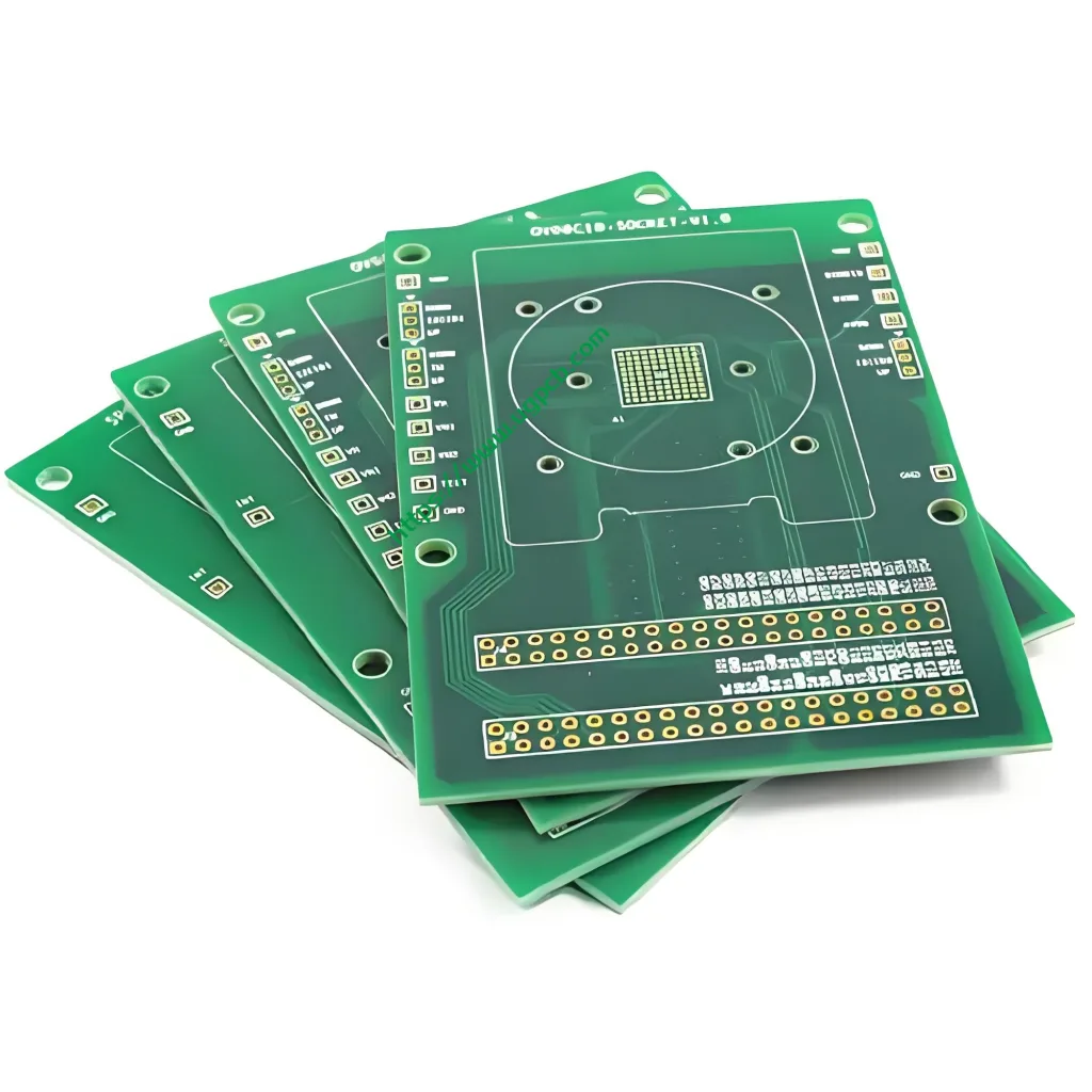
UGPCB представляет печатную плату для беспроводного пылесоса. 2-многослойная жесткая печатная плата разработан специально для портативного уборочного оборудования. Он использует Стеклоэпоксидный ламинат ФР-4 с медным плакированием в качестве основного материала. Толщина доски составляет 1,0 мм., и размеры 86.37 × 72,6 мм. Этот компактный размер идеально вписывается в ограниченное внутреннее пространство ручных и беспроводных пылесосов..
Согласно IPC-6012F Квалификационные и эксплуатационные характеристики жестких печатных плат, этот продукт подпадает под жесткая двусторонняя печатная плата (со сквозными металлизированными отверстиями) категория. В качестве ключевой части комплексной системы UGPCB печатная плата решения, этот продукт соответствует международным стандартам IPC от проектирования до производства и контроля качества.. Это обеспечивает производителям пылесосов высокую надежность., рентабельный печатная плата решение.
2. Классификация продуктов: Научное позиционирование и категоризация отраслей
Согласно IPC-6012F и стандартная печатная плата системы отраслевой классификации, этот продукт можно с научной точки зрения классифицировать следующим образом:
| Классификация Измерение | Категория |
|---|---|
| По структуре | Жесткая двусторонняя печатная плата. (со сквозными металлизированными отверстиями) |
| Базовым материалом | FR-4 эпоксидный стеклянный ламинат с медным покрытием (соответствует IPC-4101) |
| По количеству слоев | 2-слойная доска (Двусторонняя печатная плата) |
| По отделке поверхности | Бессвинцовый HASL (Выравнивание припоя горячего воздуха) |
| По классу воспламеняемости | UL 94 В-0 |
| По приложению | Потребительская электроника / плата управления небольшой бытовой техникой (пылесос PCBA) |
В отрасли электроники для пылесосов, этот продукт принадлежит кпривод двигателя и управление PCBA категория. Вместе с основной платой управления и платой управления питанием., он образует три основных модуля схемы беспроводного пылесоса.
3. Ключевые технические параметры
3.1 Основной материал и толщина платы
- Базовый материал: ФР-4 (ламинат из эпоксидной смолы, армированный стекловолокном, плакированный медью)
- Толщина доски: 1.0мм
FR-4 — наиболее широко используемая жесткая подложка в индустрии печатных плат.. Для МПК-4101, FR-4 обеспечивает превосходную электрическую изоляцию., механическая прочность, и термостойкость. Стандарт FR-4 имеет температуру стеклования. (Тг) 130–140°С. Для МПК-6012, Диапазон допуска для толщины платы 1,0 мм составляет ±0,1 мм..
3.2 Количество слоев и размеры
- Количество слоев: 2 слои (двусторонняя доска)
- Размеры: 86.37 × 72.6 мм
Двухслойная структура эффективно контролирует производственные затраты, обеспечивая при этом надежные электрические характеристики.. Это делает его основным выбором для плат управления беспроводными пылесосами.. Компактный 86.37 × Размеры 72,6 мм оптимизированы для ограниченного пространства внутри пылесоса..
3.3 Ширина трассы/интервал и минимальный размер отверстия
- Минимальный размер отверстия: 0.45мм
- Ширина трассировки/расстояние: 0.45мм / 0.391мм
Согласно IPC-2221CОбщий стандарт проектирования печатных плат, При проектировании ширины и расстояния между дорожками необходимо учитывать электрические характеристики., допустимая нагрузка по току, и производственные возможности. Минимальный размер отверстия 0,45 мм обеспечивает надежную пайку обычных DIP-компонентов и деталей со сквозными отверстиями..
По токовой нагрузке, стандартная формула отраслиЯ = k·ΔT^0,44·A^0,725 (где A — площадь поперечного сечения трассы) показывает, что с 1 унцией меди, 0,45 мм (приблизительно. 18мил) След может выдерживать ток около 1,8–2,0 А.. Плата беспроводного пылесоса использует эту ширину дорожки для сигналов привода двигателя и сигналов управления., обеспечение длительной стабильной работы.
3.4 Медная толщина фольга
- Медная толщина фольга: 1/1 ОЗ (1 унция на обоих внешних слоях)
1унция медной фольги (приблизительно. 35мкм) стандартная конфигурация для печатных плат бытовой электроники.. Он обеспечивает отличный баланс между допустимой нагрузкой по току, теплопроводность, и стоимость.
3.5 Поверхностная отделка
- Поверхностная отделка: Бессвинцовый HASL (Выравнивание припоя горячего воздуха)
HASL — это проверенное и экономичное средство для обработки поверхности печатных плат.. Бессвинцовый HASL соответствует экологическим требованиям RoHS.. По стандартам МПК, бессвинцовый HASL обычно имеет толщину слоя олова 1–40 мкм., с традиционными процессами, контролируемыми при 5–25 мкм. Эта отделка обеспечивает отличную паяемость. (смачиваемость) и хороший срок хранения до 12 месяцы.
3.6 Паяльная маска и легенда
- Спорная маска цвет: Зеленые чернила
- Цвет легенды: Белый
Зеленая паяльная маска — самый популярный выбор в отрасли.. Обеспечивает превосходную изоляционную защиту и высокую контрастность для АОИ (Автоматическая оптическая проверка). Белые надписи понятны и легко читаются., облегчение размещения компонентов и последующего обслуживания.
4. Рекомендации по проектированию: Следование стандартам IPC-2221C
Хорошо спроектированная печатная плата беспроводного пылесоса должна соответствовать этим основным принципам. (согласно IPC-2221C):
4.1 Проектирование электрических характеристик
- Ширина трассы мощности: Рассчитайте по формуле Я = k·ΔT^0,44·A^0,725 для обеспечения повышения температуры ниже 10°C при максимальном рабочем токе.
- Целостность сигнала: Используйте ширину трассы 0,45 мм для сигналов управления, чтобы гарантировать полную передачу сигналов управления скоростью ШИМ и сигналов датчиков..
- Конструкция заземления: Используйте стратегии одноточечного или раздельного заземления, чтобы предотвратить помехи силового контура контуру управления..
4.2 Проектирование терморегулирования
Беспроводные пылесосы во время работы выделяют значительное количество тепла от МОП-транзисторов.. The дизайн печатной платы должен решить эту проблему:
- Размещение тепловых массивов под силовыми устройствами.
- Расширение сильноточных дорожек или добавление открытой меди для лучшего рассеивания тепла..
- Использование плиты толщиной 1,0 мм для баланса теплопроводности и механической прочности..
4.3 Проектирование механической конструкции
The 86.37 × Размеры 72,6 мм должны точно соответствовать корпусу пылесоса.. Положения монтажных отверстий и разъемов должны соответствовать конструктивным требованиям.. Минимальный размер отверстия 0,45 мм поддерживает сквозную пайку различных DIP-компонентов и разъемов..
5. Принцип работы
Плата беспроводного пылесоса работает посредством следующих основных процессов::
① Входная мощность и управление: Литиевый аккумулятор (обычно 21,6 В или 25,2 В) проходит через схему управления питанием на печатной плате. Это обеспечивает стабильное напряжение на основной микросхеме управления и схемах драйвера..
② Вычисления основного управляющего чипа: MCU (микроконтроллер) на плате получает команды кнопок. Он рассчитывает и выводит трехфазные сигналы возбуждения с использованием FOC. (Полеориентированное управление) или алгоритмы управления прямоугольными импульсами.
③ Моторный привод: Сигналы возбуждения усиливаются силовыми устройствами MOSFET.. Эти сигналы затем приводят в действие бесщеточный двигатель постоянного тока. (БЛДК) вращаться с высокой скоростью, создание воздушного потока, необходимого для всасывания.
④ Обратная связь и защита: Печатная плата постоянно контролирует ток двигателя., напряжение батареи, температура, и другие параметры. Когда он обнаруживает аномальные условия, такие как перегрузка по току, перегрев, пониженное напряжение, или блокировка ротора, он немедленно выполняет защитные действия.
6. Материалы используются
| Компонент | Материал | Описание |
|---|---|---|
| Субстрат | Стекло эпоксидное ФР-4 | Соответствует IPC-4101 |
| Проводящий слой | Электролитическая медная фольга (1унция) | 1унция на обоих внешних слоях |
| Припаяя маска | Зеленые фотоизображенные чернила | Изоляционная защита, стойкость к окислению |
| Поверхностная отделка | Бессвинцовый сплав HASL | Соответствует RoHS |
| Легендарные чернила | Белые эпоксидные чернила | Высокая контрастность, термостойкий |
Подложка FR-4 имеет сертификат UL 94 В-0 Рейтинг воспламеняемости. В испытании на вертикальное горение, пламя гаснет внутри 10 секунд после удаления, без горящих капель. Эта функция имеет решающее значение для мощных, устройства с батарейным питанием, такие как беспроводные пылесосы. Это значительно снижает риск возгорания, вызванного неисправностями в цепи..
7. Спецификации производительности
7.1 Электрические характеристики
| Параметр | Спецификация | Справочный стандарт |
|---|---|---|
| Сопротивление изоляции | ≥10^6 МОм | МПК-6012Ф |
| Диэлектрическое выдерживаемое напряжение | До 500 В (зависит от конструкции) | МПК-2221С |
| Сопротивление проводимости | ≤50 мОм (типичный) | МПК-6012Ф |
| Характерный импеданс | Управляемый по запросу (50Ом/90 Ом/100 Ом) | МПК-2221С |
7.2 Тепловые характеристики
| Параметр | Спецификация | Справочный стандарт |
|---|---|---|
| Температура стеклянного перехода (Тг) | ≥135°С (метод ДСК) | ИПК-ТМ-650 2.4.25 |
| Теплостойкость припоя | 288°С / 10с, нет расслоения | МПК-4101 |
| Z-ось Cte (CTEz) | ≤65 частей на миллион/°C (50–260°С) | МПК-4101 |
7.3 Механические характеристики
| Параметр | Спецификация | Справочный стандарт |
|---|---|---|
| Допуск толщины платы | ±0,1 мм | МПК-6012 |
| Допуск размера отверстия | ± 0,05 мм | МПК-6012Ф |
| Рейтинг воспламеняемости | UL 94 В-0 | UL 94 |
7.4 Надежность
- Тест на паяемость: Соответствует IPC-J-STD-003
- Тест на старение: 500 часов в условиях двойного-85 (85°С / 85%Раствор) без отклонений
8. Структурные особенности
8.1 2-Преимущества многослойной платы
Верхний слой содержит основные компоненты и следы сигналов.. Нижний слой предназначен для вспомогательных компонентов и заливки меди заземления/питания.. Двухслойная конструкция обеспечиваетлучшая цена ивысочайшая надежность баланс для функций управления беспроводным пылесосом.
8.2 Позолоченное сквозное отверстие (ПТХ) Процесс
Во всех сквозных отверстиях используется технология сквозных отверстий с металлическим покрытием.. Это обеспечивает надежную взаимосвязь между верхним и нижним слоями.. Он также обеспечивает надежную механическую поддержку и электрическое соединение для компонентов DIP..
8.3 Процесс моста с паяльной маской
Зеленая паяльная маска образует перемычки между соседними контактными площадками.. Это предотвращает спаивание коротких замыканий и повышает выход SMT-размещения..
9. Схема производственного процесса
UGPCB строго следует стандартам IPC-6012F для контроля каждого этапа производства.:
① Входной контроль материалов →② Создание схемы внутреннего слоя. (для двухслойных плат, это непосредственно внешний слой) →③ Ламинирование (не применимо для 2-слойных плат) →④ Сверление (минимальный размер отверстия 0,45 мм) →⑤ Химическое осаждение меди / Панельное покрытие →⑥ Схема внешнего слоя →⑦ Узорчатое покрытие →⑧ Травление →⑨ Паяльная маска (зеленые чернила) →⑩ Обработка поверхности (бессвинцовый HASL) →⑪ Легенда (белые персонажи) →⑫ Маршрутизация профиля (86.37 × 72,6 мм) →⑬ Электрические испытания →⑭ Заключительная проверка (для IPC-A-600) →⑮ Упаковка и доставка
Каждая партия проходитТестирование летающих зондов илиспециальное тестирование приспособлений чтобы обеспечить 100% отсутствие обрывов и коротких замыканий.
10. Сценарии приложения
10.1 Основные приложения
- Ручные беспроводные пылесосы: Моторный привод и управление в компактных помещениях
- Аккумуляторные пылесосы в стиле палки: Управление аккумулятором и бесщеточный моторный привод
- Роботы-пылесосы: Навигационное управление и моторный привод
- Автомобильные пылесосы: 12Адаптация и управление питанием В/24 В
- Умные устройства для уборки: Подключение к Интернету вещей и интеллектуальное управление
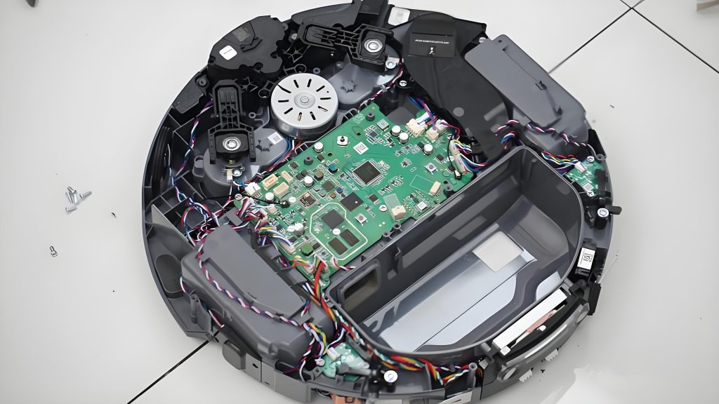
10.2 Примеры конечного продукта
Эту печатную плату можно широко использовать в платах управления и платах драйверов беспроводных пылесосов и аналогичных чистящих устройств таких брендов, как Xiaomi., Дайсон, Тинеко, и Лейфхайт.
11. Почему стоит выбрать печатную плату беспроводного пылесоса UGPCB?
✅Соответствие международным стандартам: Дизайн, Производство, и проверка полностью соответствуют IPC-6012F, МПК-А-600, МПК-2221С, и другие международные стандарты
✅УЛ 94В-0 Пожарная безопасность: Подложка FR-4 обеспечивает высочайшую степень вертикального горения., обеспечение безопасности устройства

✅Бессвинцовый экологически чистый процесс: Бессвинцовая поверхность HASL соответствует экологическим директивам RoHS и REACH.
✅Проверенные производственные возможности: UGPCB предоставляет комплексные услуги от проектирования и производства печатных плат до сборки печатных плат.
✅Строгий контроль качества: Визуальный осмотр согласно IPC-A-600 и 100% электрические испытания обеспечивают качество отгрузки
✅Компактные оптимизированные размеры: The 86.37 × Размер 72,6 мм идеально вписывается во внутреннее пространство различных беспроводных пылесосов.
12. Получите ценовое предложение и образцы сегодня
УГКПБ стремится обеспечить высокую точность, высоконадежные решения для печатных плат и печатных плат для производителей электроники по всему миру. Нужен ли вам голые печатные платы, полностью собранная печатная плата, или Комплексные услуги от проектирования до массового производства, У UGPCB есть опыт, который поможет вам.
📧Свяжитесь с UGPCB для получения индивидуального предложения сегодня →
- Веб-сайт: www.ugpcb.com
- Доступны индивидуальные модификации и оптимизации дизайна.
- Бесплатный ДФМ (Дизайн для производства) обзор
- Доступны как быстрое прототипирование, так и серийное производство.
Декларация источника данных
Технические стандарты и данные, приведенные в этой статье, получены от следующих авторитетных организаций.:
- МПК (Ассоциация, объединяющая электронную промышленность): МПК-6012Ф Квалификационные и эксплуатационные характеристики жестких печатных плат, МПК-А-600 Приемлемость печатных плат, МПК-2221С Общий стандарт проектирования печатных плат, МПК-4101 Спецификация базовых материалов для жестких и многослойных печатных плат, ИПК-ТМ-650 Руководство по методам испытаний
- UL (Андеррайтеры лаборатории): UL 94 Стандарт на безопасность воспламеняемости пластмассовых материалов для деталей устройств и приборов – В-0 рейтинг
- Стандартная инженерная формула отрасли: Формула допустимой нагрузки по току печатной платы Я = k·ΔT^0,44·A^0,725













