

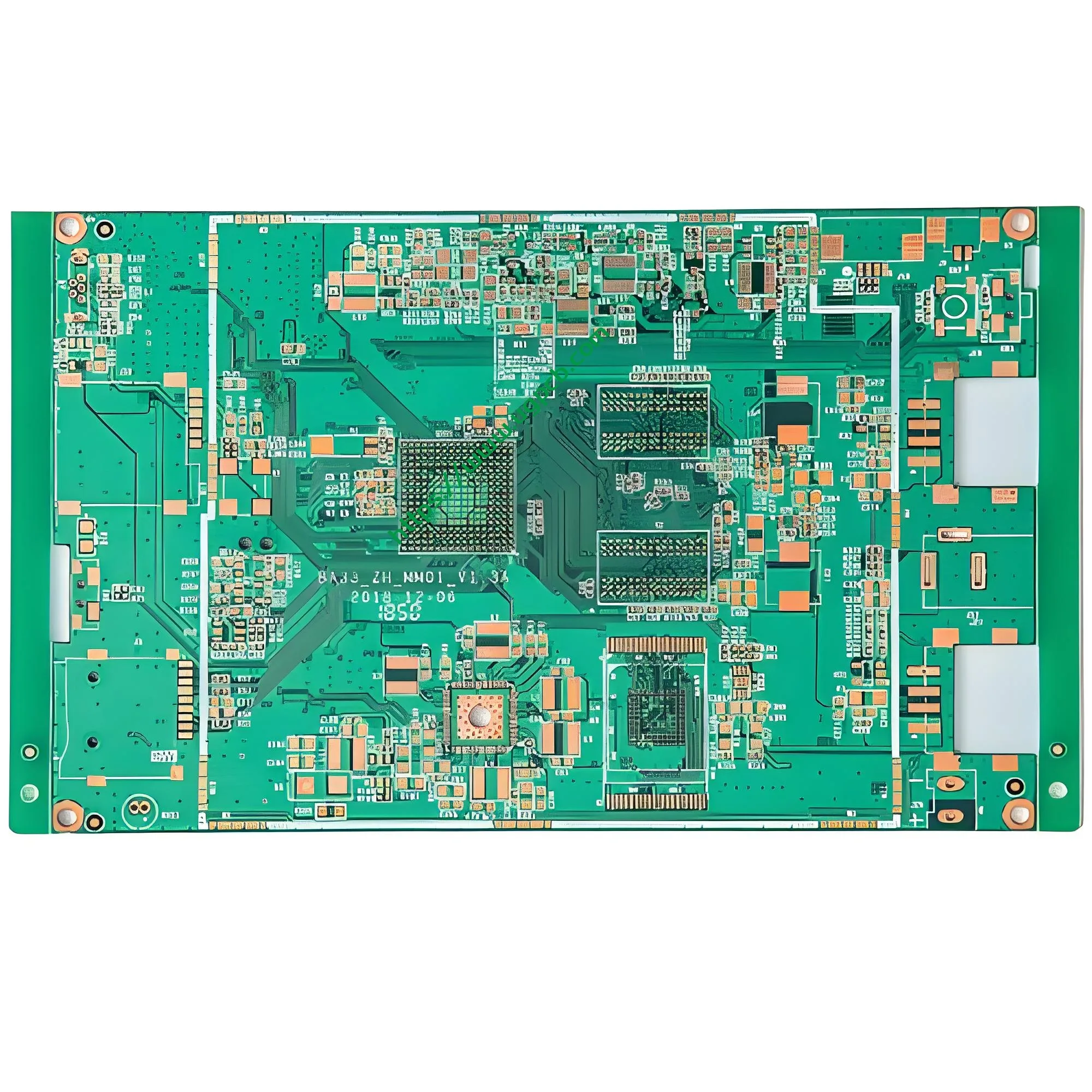
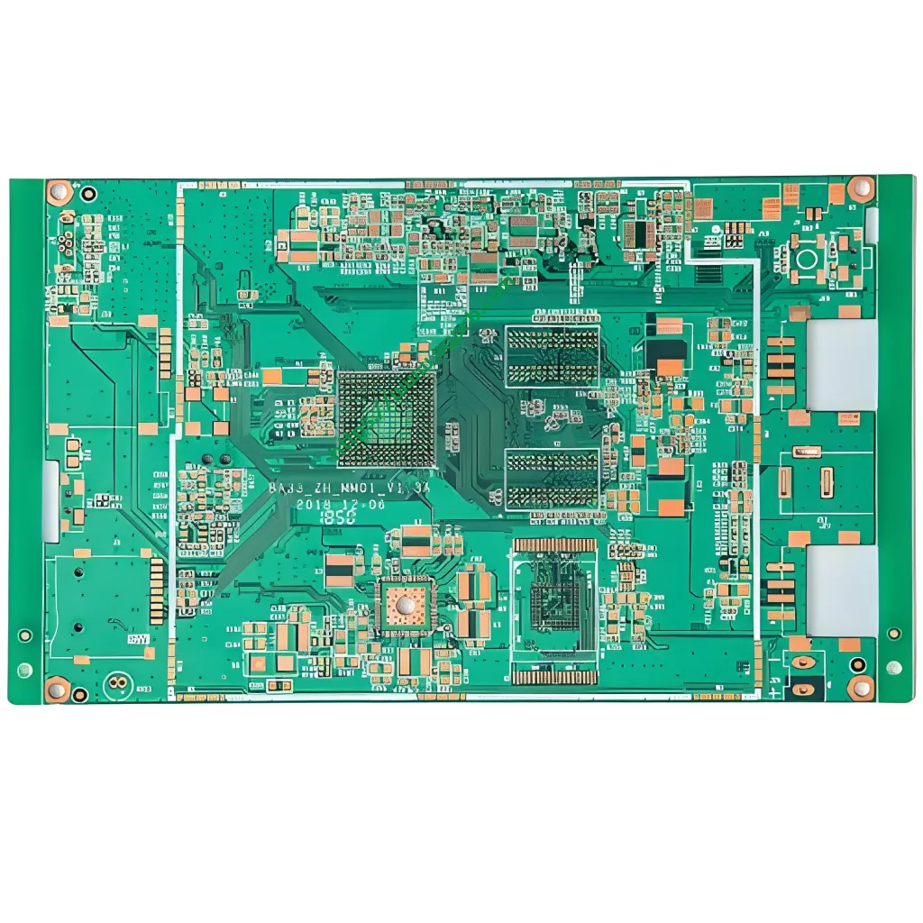
Обзор продукта: Что такое печатная плата с антиоксидантом OSP?
АнПечатная плата антиоксидантной печатной платы OSP ИспользованиеОрганическая припаяя консерванты (ОСП) как его медная отделка поверхности. В результате этого процесса на голых медных поверхностях образуется ультратонкая органическая пленка.. Пленка предотвращает окисление при хранении и сборке.. Во время пайки, флюс быстро растворяет пленку ОСП. Это обнажает чистую медь для надежных паяных соединений..
В печатной плате UGPCB OSP с антиоксидантами используютсяСтеклоэпоксидный ламинат ФР-4 в качестве основного материала. Он имеет размер 35 мкм. (1 унция) медная фольга, 1.6мм толщина доски, и размеры 68.36 × 34,6 мм. Минимальный размер готового отверстия составляет 0,45 мм.. Минимальная ширина дорожки — 0,15 мм, минимальный интервал — 0,20 мм.. Продукт полностью соответствует стандарту IPC-6012E. (квалификация и производительность жесткой печатной платы) и МПК-4555 (высокотемпературные характеристики OSP) спецификации.
Этотдвусторонняя печатная плата OSP обслуживает бытовую электронику, оборудование связи, и промышленный контроль. Он лучше всего работает там, где важнее всего экономическая чувствительность и плоскостность поверхности..
Классификация научной продукции
На основе международной системы классификации печатных плат., этот продукт попадает в эти категории:
| Классификация Измерение | Категория |
|---|---|
| Материал подложки | Жесткая печатная плата из эпоксидной стеклоткани FR-4 |
| Количество слоев | Двусторонний (двухслойная схема) |
| Поверхностная отделка | ОСП (Органическая припаяя консерванты) антиоксидант |
| Рейтинг воспламеняемости | UL 94 В-0 |
| Класс производительности МПК | Сорт 2 (электронные продукты для специального обслуживания) |
| Медная толщина фольга | 1 унция (35мкм) стандартная медь |
| Толщина доски | 1.6мм стандартная жесткая плита |
| Тип отверстия | Сквозное отверстие, совместимое с SMT |
Объяснение ключевых технических параметров
Субстрат: Эпоксидная стеклоткань FR-4
FR-4 — наиболее распространенная жесткая подложка в печатная плата промышленность. “фр.” значит огнестойкий. “4” указывает на эпоксидную смолу в сочетании со стеклотканью, которая соответствуетUL 94 В-0 стандарты воспламеняемости. UL 94 В-0 требует, чтобы вертикальные образцы самозатухали в пределах10 секунды после двух 10-секундных воздействий пламени. Никакие горящие капли не могут воспламенить хлопок..

Температура стеклования (Тг) измеряет термостойкость. Стандартный диапазон Tg FR-4 составляет 130–140°C.. Средняя Tg FR-4 достигает 150–160°С.. Высокая Tg FR-4 превышает 170°C. В этом продукте используется стандарт FR-4 с Tg ≥ 130°C. (Соответствует IPC-4101/21). Это соответствует требованиям к термическому удару, предъявляемым к пайке оплавлением. (пиковые температуры 240–260°C).
Медная толщина фольга: 35мкм (1 унция)
Толщина меди определяет допустимую токовую нагрузку. Этот продукт использует35мкм медная фольга, известный как1 Оз меди (1 унция/фут² ≈ 35 мкм). Согласно МПК-2221, 1 унция меди при повышении температуры на 10°C содержит примерно:
- 0.15мм (6 мил) Ширина следа: 0.5-0,7А
- 0.20мм (8 мил) Ширина следа: 0.8-1,0 А
Толщина меди 35 мкм является наиболее распространенным стандартом для двусторонних печатных плат.. Это уравновешивает стоимость, текущая мощность, и выход продукции.
Размеры платы: 68.36 × 34,6 мм
Готовая доска имеет размеры68.36мм × 34,6 мм. Этот компактный размер подходит для компактных электронных модулей.. Маленькие печатные платы требуют более высокой точности — допуски на размеры обычно остаются в пределах ±0,15 мм. (IPC-6012 Класс 2).
Минимальный размер готового отверстия: 0.45мм
0.45мм минимальное металлизированное сквозное отверстие (ПТХ) диаметр. Этот размер отверстия является стандартом в отрасли.. Обеспечивает надежное покрытие. (соотношение сторон приблизительно 3.6:1 с толщиной доски 1,6 мм.). Размер отверстия подходит для большинства компонентов DIP и стандартных конструкций площадок SMT..
Толщина печатной платы: 1.6мм
1.6мм — наиболее распространенная толщина платы при производстве печатных плат.. Обеспечивает превосходную механическую прочность и жесткость на изгиб.. Идеально сочетается со стандартными разъемами и гнездами..
Ширина следа и расстояние: 0.15мм / 0.20мм
Этот продукт предлагаетминимальная ширина дорожки 0,15 мм (о 6 мил) иминимальное расстояние 0,20 мм (о 8 мил). По классификации МПК, эти размеры попадают вСорт 2 (электронные продукты для специального обслуживания). Такая точность соответствует большинству конструкций печатных плат средней плотности., включая платы управления MCU, модули управления питанием, и платы преобразователя интерфейсов.
Как работает антиоксидантный процесс OSP
В процессе OSP на чистой голой меди образуется ультратонкая органическая пленка.химическая адсорбция. Фильм OSP в основном состоит изалкилбензимидазольные соединения (на основе азола). Толщина пленки обычно колеблется от0.2–0,5 мкм.
Механизм защиты
Пленка OSP защищает медные поверхности посредством трех механизмов.:
- Физический барьер – Органическая пленка образует плотный молекулярный слой. Он блокирует контакт кислорода и влаги с медной поверхностью..
- Химическая адсорбция – Активные группы в молекулах OSP химически связаны с атомами меди.. Это создает прочную адгезию.
- Выборочная защита – Пленка OSP покрывает только медные участки. Не влияет на паяльную маску или другие неметаллические участки..
Поведение во время пайки
Во время оплавления SMT, температура достигает190–230°С. Активные ингредиенты флюса разлагают и растворяют пленку OSP.. Это обнажает чистую медь под ней.. Припой непосредственно контактирует с голой медью и образуетинтерметаллические соединения (IMC). Это создает надежные электрические соединения.. фильм «ОСП»полностью разлагается без остатков после пайки.
Ключевые характеристики производительности
На основе методов испытаний IPC-TM-650.:
| Характеристика | Типичное значение / Требование | Справочный стандарт |
|---|---|---|
| Толщина пленки OSP | 0.2–0,5 мкм | МПК-4555 |
| Угол смачивания припоя | ≤30° (после 1 переиз) | ИПК-ТМ-650 2.4.1 |
| Коэффициент распространения припоя | ≥80% | ИПК-ТМ-650 2.4.1 |
| Защита от окисления (окружающий) | ≥6 месяцев | МПК-4555 |
| Изменение контактного сопротивления | ≤10% (после 6 месяцы хранения) | ИПК-ТМ-650 |
Процесс производства антиоксидантных печатных плат OSP
Производство печатных плат с антиоксидантами OSP следует строгому технологическому контролю.. Каждый шаг влияет на конечное качество и надежность.
Внешние процессы (Подготовка субстрата & Паттерн схемы)
- Материальная резка – Отрезать медный ламинат FR-4 по размеру.
- Бурение – Сверление на станке с ЧПУ с минимальным размером отверстия 0,45 мм.
- Химическое медь / Гальваника – Металлизировать стенки отверстий для послойного соединения
- Передача шаблона схемы — Сухая пленка / экспонирование и проявление влажной пленки
- Офорт – Удалите ненужную медь, чтобы создать дорожку толщиной 0,15 мм. / 0.20схема расстояния в мм
- Печать паяльной маски – Нанесите зеленые или другие цветные чернила для паяльной маски.
- Предварительная очистка – Удалите оксиды и загрязнения перед финишной отделкой поверхности.
Процесс нанесения покрытия OSP (Основной процесс)
Типичный процесс нанесения покрытия OSP:
Обезжиривание → Двойная промывка водой → Микротравление → Двойная промывка водой → Травление кислотой → Промывка деионизированной водой → Формирование пленки OSP → Сушка на воздухе → Промывка деионизированной водой → Окончательная сушка
- Микротравление – Удаляет оксиды меди и создает однородную микроскопически шероховатую поверхность.. Это способствует росту пленки OSP..
- Формирование фильма ОСП – Погрузите печатную плату в химию OSP. (алкилбензимидазол, органические кислоты, хлорид меди, и деионизированная вода). Пленка растет за счет химической адсорбции на медных поверхностях..
- Контроль толщины пленки – Точный контроль имеет решающее значение. Слишком тонкий означает плохую термостойкость.. Слишком толстый слой препятствует действию флюса и растеканию припоя..
Внутренние процессы
- Маршрутизация – Фрезерование на станке с ЧПУ до окончательных размеров
- Электрические испытания – Тестирование летающего зонда или приспособления
- Заключительная проверка – Визуальный осмотр и отбор проб толщины пленки
- Вакуумная упаковка – Влагостойкая и устойчивая к окислению упаковка.
Особенности продукта и основные преимущества
Отличная плоскостность поверхности
Фильм OSP только0.2–0,5 мкм толстый. Он образуется за счет химической адсорбции с одинаковой толщиной и гладкой поверхностью.. Это сохраняет первоначальную плоскостность медной фольги.. Он идеально подходит длямелкий шаг SMT компоненты (например, QFP с шагом 0,4 мм и ниже, QFN-пакеты).
Превосходная паяемость
Пленка OSP быстро растворяется во флюсе во время оплавления.. Это обнажает свежую медь для надежного формирования IMC.. Процесс OSP поддерживает обасквозное отверстие (ТТТ) иповерхностный монтаж (СМТ) пайрь.
Экономичный
OSP не использует драгоценные металлы (золото, серебро, палладий). Затраты на материалы и обработку ниже, чем у ENIG., погружение серебро, или иммерсионная банка. Для крупносерийного производства, например бытовой электроники., OSP предлагает исключительную конкурентоспособность затрат.
Экологичность
OSP использует органические соединения.. Он не содержит свинца, Меркурий, кадмий, или шестивалентный хром. Оно полностью соответствуетRohs 2.0 требования. Затраты и сложность переработки отходов также ниже, чем при обработке металлов..
Короткое время обработки
Покрытие OSP – это просто и быстро. Для этого не требуется сложное оборудование для нанесения покрытия или длительное время осаждения.. По сравнению с ЭНИГ (что занимает несколько часов), OSP завершает отделку поверхности в30–60 минут за партию. Это значительно сокращает время выполнения заказов.
Рекомендации по проектированию и важные соображения
Дизайн для производства (DFM) Правила
На основе технологических возможностей данного продукта:
| Проектный параметр | Возможности продукта | Рекомендуемое расчетное значение |
|---|---|---|
| Минимальная ширина трассировки | 0.15мм | ≥0,15 мм (следы сигнала) |
| Минимальный интервал | 0.20мм | ≥0,20 мм |
| Минимальный размер отверстия | 0.45мм | ≥0,45 мм |
| Толщина доски | 1.6мм | 1.6мм (стандартный) |
Ограничения процесса OSP и их смягчение
OSP предлагает множество преимуществ, но имеет присущие ограничения.:
- Ограниченный срок годности – Пленка OSP защищает6 месяцы в условиях окружающей среды. Для лучшей паяемости, полная сборка SMT в течение 3 месяцы.
- Чувствительность к влаге – Пленки OSP разрушаются при высоких температурах., среда с высокой влажностью. Храните доски по адресу20–25°C при относительной влажности 40–60 %..
- Ограниченные циклы оплавления – Стандартный OSP выдерживает1–2 термические удары оплавлением. Множественные оплавления требуют высокотемпературного OSP. (Соответствует IPC-4555).
- Проблемы электрических испытаний – Пленка ОСП изолирующая. Это влияет на надежность электрических испытательных контактов.. Для контрольных точек требуется печать паяльной пасты для удаления слоя OSP..
Рекомендации по хранению и обращению
- Вакуумная упаковка с карточками влагопоглотителя и индикатора влажности.
- Среда хранения: температура ≤30°С, относительная влажность ≤60%
- Полная пайка внутри48 часы открытия пакета
- Во время работы надевайте антистатические перчатки.. Избегайте контакта голых рук с поверхностями доски..
Типичные сценарии применения
Печатные платы OSP с антиоксидантами используются во многих отраслях промышленности благодаря своимценовое преимущество, плоскостность поверхности, и отличная паяемость:
Бытовая электроника
- Материнские платы для смартфонов и печатные платы для планшетов
- Компьютерные материнские платы и видеокарты
- Платы управления бытовой техникой
- Печатные платы носимых устройств
Коммуникационное оборудование
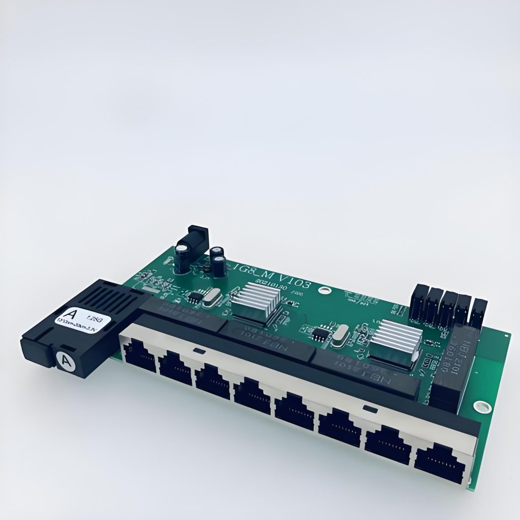
- Платы маршрутизатора и коммутатора
- Модули связи и устройства IoT
- Bluetooth / Платы-носители модулей Wi-Fi
Промышленный контроль
- Программируемые логические контроллеры ПЛК
- Модули управления питанием
- Платы приборов
- Платы управления электроприводом
Автомобильная электроника (Некритичные для безопасности)
- Автомобильные информационно-развлекательные системы
- Модули управления кузовом
- Платы интерфейса датчиков
Гарантия качества и соответствие стандартам
Применимые стандарты
Антиоксидантный продукт для печатных плат OSP компании UGPCB строго соответствует этим международным стандартам.:
| Стандартный | Заголовок | Объем |
|---|---|---|
| МПК-4555 | Технические характеристики высокотемпературных органических консервантов для пайки (ОСП) для печатных плат | Требования и тестирование процесса OSP |
| IPC-6012E | Квалификационные и эксплуатационные характеристики жестких печатных плат | Качество и производительность готовой платы |
| МПК-4101/21 | Спецификация на эпоксидный ламинат, армированный стекловолокном | Технические требования к подложке FR-4 |
| ИПК-ТМ-650 | Руководство по методам испытаний | Различные методы тестирования производительности |
| UL 94 В-0 | Воспламеняемость пластиковых материалов | Огнезащитная безопасность основания |
| Rohs 2.0 | Ограничение использования опасных веществ | Экологическое соответствие |
Ключевые показатели качества
Согласно требованиям МПК, Ключевые показатели качества включают в себя:
- Толщина пленки OSP: 0.2–0,5 мкм, допуск на однородность ≤ ± 0,1 мкм
- Адгезия: ≥4Б (ИПК-ТМ-650 2.4.29 поперечный тест)
- Коэффициент распространения припоя: ≥80% (ИПК-ТМ-650 2.4.1)
- Период защиты от окисления: ≥6 месяцев (условия окружающей среды)
- Рейтинг воспламеняемости: UL 94 В-0
Почему стоит выбрать UGPCB для антиоксидантных печатных плат OSP?
Возможности точного производства
- 0.15минимальная ширина трассы, мм / 0.20минимальное расстояние мм
- 0.45мм минимальный размер готового отверстия
- 1.6стандартная толщина плиты мм с отличной совместимостью
Надежное управление процессами OSP
- Строгое соблюдение стандарта IPC-4555 по толщине и качеству пленки.
- Полная отслеживаемость на протяжении всего производственного процесса.
- Тестирование паяемости и отбор проб толщины пленки для каждой партии
Быстрая доставка
- Стандартное время выполнения: 7–10 рабочих дней
- Поддерживает как выборку прототипов, так и серийное производство.
Комплексная техническая поддержка
- Бесплатный обзор дизайна DFM
- Профессиональная команда инженеров для руководства по выбору продукции
Получите предложение сегодня
UGPCB поставляет высококачественные решения для печатных плат OSP с антиоксидантами. Нужен ли вамвыборка прототипа илиобъем производства, мы обеспечиваем профессиональную техническую поддержку и конкурентоспособные цены.
📞 Как получить ценовое предложение:
- Отправьте файлы Gerber и список спецификаций
- Наша команда инженеров ответит индивидуальным решением и ценой в течение24 часы
- Бесплатная проверка DFM, чтобы убедиться, что ваш проект прошел проверку с первого раза
Заявление об источнике данных: Технические данные и стандартные требования, указанные в этом документе, в первую очередь взяты из IPC. (Ассоциация, объединяющая электронную промышленность) стандарты, включая IPC-4555 “Технические характеристики высокотемпературных органических консервантов для пайки (ОСП) для печатных плат,” IPC-6012E “Квалификационные и эксплуатационные характеристики жестких печатных плат,” МПК-4101/21 “Спецификация на эпоксидный ламинат, армированный стекловолокном,” ИПК-ТМ-650 “Руководство по методам испытаний,” и UL 94 “Стандарт на испытания на воспламеняемость пластмассовых материалов для деталей устройств и приборов.” Некоторые параметры процесса ссылаются на общедоступные технические данные ведущих производителей печатных плат.. Все данные проверены на достоверность.













