

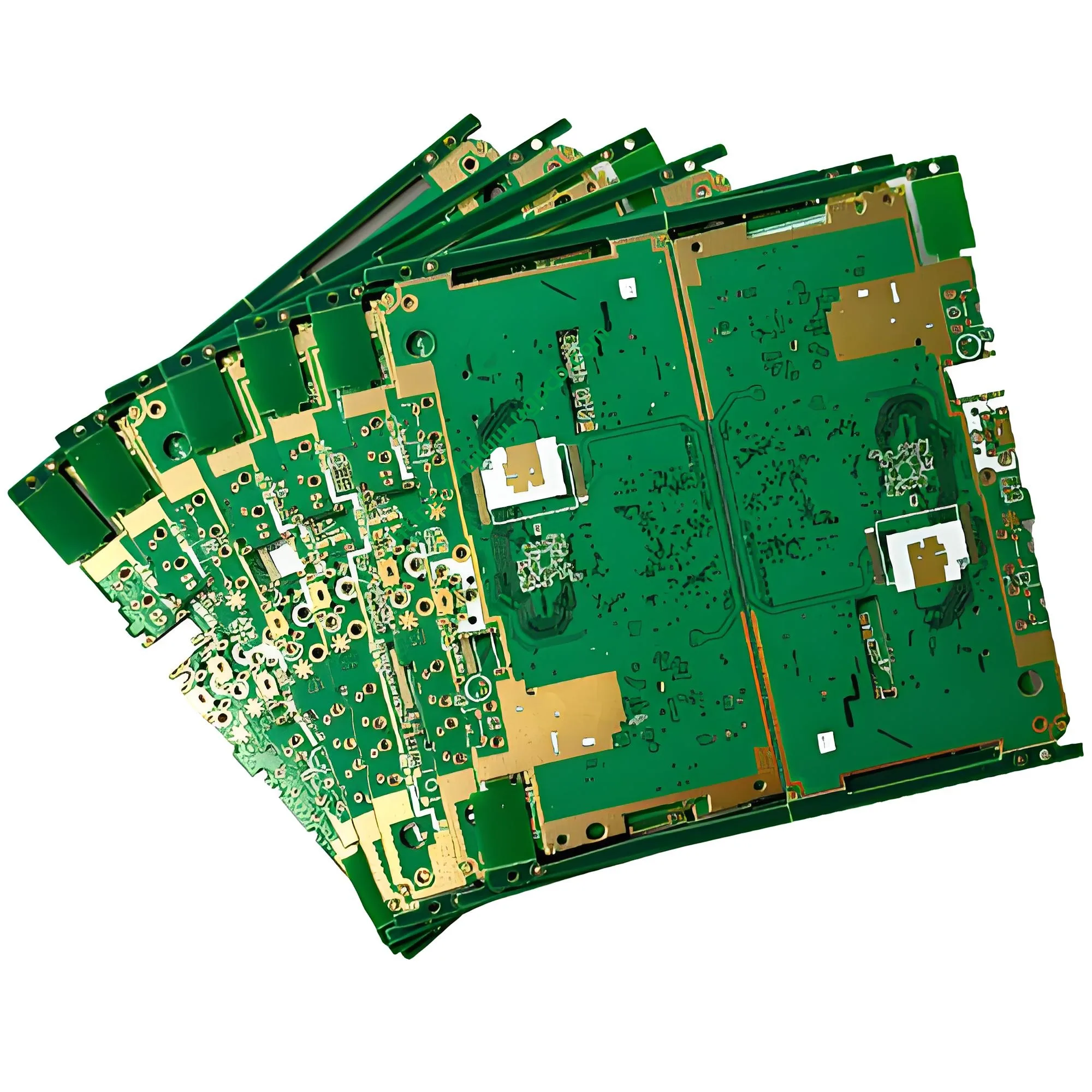
я. Обзор продукта: Печатная плата, разработанная для беспроводных систем дверных звонков
Печатная плата беспроводного дверного звонка является важным электронным компонентом в системах умного дома и безопасности.. UGPCB предлагает эту плату, изготовленную из высокопроизводительного ламината Kingboard KB6165F с медным покрытием.. Производственный процесс проходит строгий контроль качества..
Эта печатная плата беспроводного дверного звонка представляет собой двухслойную двустороннюю плату. печатная плата. Он имеет толщину 1,0 мм и размеры 79.48 × 35,6 мм. Эти размеры идеально подходят для компактных корпусов беспроводных дверных звонков.. На плате используется бессвинцовый HASL. (Выравнивание припоя горячего воздуха) обработка поверхности. Это покрытие соответствует экологическим требованиям RoHS и обеспечивает превосходную паяемость..
Беспроводные дверные звонки служат первой линией защиты в домашней безопасности.. Надежность их печатных плат напрямую определяет срок службы продукта и удобство использования.. УГКПБ понимает это критическое требование. Мы тщательно выбираем материалы и контролируем каждый этап процесса, чтобы обеспечить высококачественный беспроводной дверной звонок. Печатные платы клиентам по всему миру.
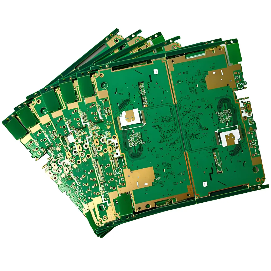
II. Определение продукта и позиционирование в отрасли
АПечатная плата беспроводного дверного звонка это печатная плата, используемая в системах беспроводных дверных звонков.. Обычно он состоит из двух частей: плата передатчика и плата приемника. Печатная плата передатчика содержит чип энкодера. (например HT12E), модуль беспроводного передатчика 433 МГц, и схема кнопочного переключателя. Печатная плата приемника содержит чип декодера. (например HT12D), модуль беспроводного приемника, аудиоусилитель, и схема драйвера динамика.
С точки зрения классификации печатных плат, этот продукт являетсяжесткая двусторонняя печатная плата (Жесткая двусторонняя печатная плата) . Его можно дополнительно классифицировать следующим образом:
| Классификация Измерение | Категория |
|---|---|
| Проводящие слои | Двусторонний (2л) |
| Жесткость подложки | Жесткая доска |
| Поверхностная отделка | Бессвинцовый HASL |
| Рейтинг воспламеняемости | UL 94 В-0 |
| Класс производительности МПК | Сорт 2 (Электронные продукты, предназначенные для специального обслуживания) |
Этот продукт соответствует стандарту IPC-6012.Квалификационные и эксплуатационные характеристики жестких печатных плат. Материал его подложки, КБ6165F, соответствует требованиям спецификации IPC-4101/99.
III. Ключевые технические параметры
3.1 Материал подложки: Ламинат Kingboard KB6165F с медным покрытием
KB6165F — этобессвинцовый стеклотекстолит Tg150, плакированный медью ламинат производства Kingboard Laminates Holdings Limited.. Он относится к семейству эпоксидных стеклотканевых ламинатов класса FR-4.. Ключевые показатели эффективности следующие::
- Температура стеклянного перехода (Тг) : 154°С (Метод испытания: ИПК-ТМ-650 2.4.25)
- Z-ось Cte (Коэффициент термического расширения) : 40 ppm/° C. (50–260°С), полное расширение 3.1% (Метод испытания: ИПК-ТМ-650 2.4.24)
- T-288 Время расслоения : >30 минуты (Метод испытания: ИПК-ТМ-650 2.4.24.1)
- Температура термического разложения (Тд, 5% потеря веса) : 346°С (Метод испытания: ИПК-ТМ-650 2.4.24.6)
- Рейтинг воспламеняемости : UL 94 В-0
- Диэлектрическая проницаемость (Дк) @ 1 ГГц : 4.6 (Метод испытания: ИПК-ТМ-650 2.5.5.2)
- Коэффициент рассеяния (Дф) @ 1 ГГц : 0.016 (Метод испытания: ИПК-ТМ-650 2.5.5.2)
- Прочность на очистку (1 унция медной фольги) : 1.4 N/мм (Метод испытания: ИПК-ТМ-650 2.4.8)
- Прочность на гибкость : 550 Н/мм² (продольный) / 485 Н/мм² (поперечный) (Метод испытания: ИПК-ТМ-650 2.4.4)
- Влажно -поглощение : 0.10% (Метод испытания: ИПК-ТМ-650 2.6.2.1)
- Термический стресс : ≥240 секунд (Метод испытания: ИПК-ТМ-650 2.4.13.1)
Высокий ТГ (>150°С) означает, что эта подложка может выдерживать высокие температуры процессов бессвинцовой пайки. Эффективно предотвращает коробление и расслоение доски во время сборки.. Это отличный анти-CAF (Проводящая анодная нить) производительность обеспечивает надежность во влажной среде и в условиях длительного включения питания.
3.2 Толщина платы и количество слоев
Толщина доски составляет1.0мм с2 слои (2л) . Такая толщина обеспечивает достаточную механическую прочность, одновременно удовлетворяя требованиям к тонкому и компактному дизайну беспроводных дверных звонков.. Двухслойная конструкция обеспечивает правильную компоновку радиочастотных цепей., силовые цепи, и схемы управления на платах передатчика и приемника.. Это оптимизирует целостность сигнала и целостность питания..
3.3 Размеры
Размеры79.48мм × 35,6 мм. Этот компактный размер оптимизирован для внутреннего пространства беспроводных дверных звонков.. Он вмещает все функциональные схемы и легко вписывается в различные корпуса дверных звонков..
3.4 Минимальная апертура
Минимальная апертура0.332мм. Согласно требованиям IPC-6012 для сквозных металлизированных отверстий., этот размер отверстия отвечает требованиям надежности при вставке выводов компонентов и благодаря металлизации в печатных платах беспроводных дверных звонков..
3.5 Ширина следа и расстояние
Ширина следа0.42мм и расстояние между следами0.46мм. Согласно МПК-2221Общий стандарт проектирования печатных плат, токовую нагрузку можно рассчитать по следующей формуле:
Где:
- = Максимальная допустимая нагрузка по току (амперы)
- = Поправочный коэффициент (0.048 для внешних слоев, 0.024 для внутренних слоев)
- = Допустимое повышение температуры (°С)
- = Площадь поперечного сечения проводника (квадратный мил)
Для следов внешнего слоя с 1 унция медной фольги (1.37 милы толщиной) и ширина дорожки 0,42 мм. (примерно 16.5 мил), площадь поперечного сечения:
При повышении температуры на 10°С, теоретическая допустимая нагрузка по току равна:
Эта мощность тока полностью соответствует требованиям маломощных радиочастотных цепей и цепей цифрового управления в печатных платах беспроводных дверных звонков..
3.6 Медная толщина фольга
Толщина медной фольги составляет1/1ОЗ (1 унция на обоих внешних слоях, примерно 35 мкм). Такая толщина обеспечивает превосходный баланс между допустимой нагрузкой по току., теплопроводность, и стоимость. Это стандартная конфигурация для печатных плат бытовой электроники..
3.7 Поверхностная отделка: Бессвинцовый HASL
Отделка поверхностибессвинцовый HASL (Выравнивание припоя горячего воздуха) . В этом процессе, Печатная плата погружена в расплавленный бессвинцовый припой. (обычно Sn99.3Cu0.6). Затем ножи горячего воздуха под высоким давлением продувают поверхность, чтобы удалить излишки припоя..
Ключевые преимущества бессвинцовой отделки поверхности HASL включают в себя::
- Отличная паяемость : Подходит для нескольких циклов пайки.
- Длительный срок хранения : Припой обеспечивает хорошую стабильность при хранении.
- Экономическая эффективность : Более экономичный, чем ENIG и другие варианты отделки.
- Соответствие RoHS : Не содержит свинца и других запрещенных веществ.
Эта обработка поверхности соответствует требованиям к покрытию, указанным в IPC-6012..
3.8 Паяльная маска и легенда
Паяльная маска естьзеленые чернила и легендабелые чернила. Зеленая паяльная маска — самый популярный выбор в индустрии печатных плат.. Обладает отличными изоляционными свойствами., теплостойкость, и визуальная ясность. Белая легенда гарантирует, что обозначения компонентов, метки полярности, и другая информация остается четко читаемой.
IV. Рекомендации по проектированию и принципы работы
4.1 Рекомендации по проектированию
Беспроводной дверной звонок дизайн печатной платы требует внимания к нескольким критическим областям:
(1) Проектирование радиочастотных схем
Беспроводные дверные звонки обычно работают в диапазоне ISM 433 МГц.. Радиочастотные трассы должны быть спроектированы как микрополосковые линии с характеристическим сопротивлением 50 Ом или копланарные волноводы.. Ширина трассы должна быть точно рассчитана на основе Материал печатной платы параметры (Dk = 4.6). Антенну следует размещать рядом с краем печатной платы.. Не размещайте его в середине платы и не окружайте его большими плоскостями заземления..
(2) Целостность власти
Цепи управления питанием на платах передатчика и приемника требуют правильной компоновки.. Разместите развязывающие конденсаторы рядом с выводами IC, следуя инструкциям. “близкие и множественные” принцип.
(3) Уменьшение помех
Поместите схему приемника в угол печатной платы., вдали от импульсных источников питания и других источников шума. Схема кварцевого генератора нуждается в собственной земле и должна располагаться как можно ближе к микроконтроллеру..
(4) Тепловое управление
Толщина доски 1,0 мм в сочетании с 1 медная фольга на унцию обеспечивает хорошую теплопроводность. Это эффективно рассеивает тепло от усилителей мощности RF и других компонентов, выделяющих тепло..
4.2 Принципы работы
Беспроводная система дверного звонка состоит из передатчика и приемника.:
Работа передатчика : Когда пользователь нажимает кнопку дверного звонка, чип кодера (например HT12E) на плате передатчика кодирует сигнал кнопки. Модуль радиочастотного передатчика 433 МГц затем отправляет этот закодированный сигнал по беспроводной сети.. Во время работы передатчик обычно потребляет ток около 5,6 мА..
Работа приемника : Модуль радиочастотного приемника 433 МГц на плате приемника постоянно отслеживает беспроводные сигналы.. Когда он получает соответствующий закодированный сигнал, чип декодера (например HT12D) декодирует это. Это запускает схему аудиоусилителя, которая приводит в действие динамик и воспроизводит звуковой сигнал дверного звонка..
В. Особенности продукта и преимущества производительности
5.1 Особенности продукта
| Особенность | Описание |
|---|---|
| Высоконадежная подложка | Ламинат Kingboard KB6165F Tg150, UL 94 В-0 огнестойкий |
| Экологически чистый бессвинцовый процесс | Бессвинцовая обработка поверхности HASL, Соответствует RoHS |
| Возможности точного производства | Минимальная апертура 0,332 мм, поддерживает маршрутизацию высокой плотности |
| Отличная термостойкость | T-288 >30мин, выдерживает температуры бессвинцовой пайки оплавлением |
| Превосходные электрические характеристики | Дк=4,6, Df=0,016 @ 1 ГГц, подходит для радиочастотных применений |
| Высокая точность размеров | Точные размеры 79,48×35,6 мм., подходит для стандартных корпусов дверных звонков |
5.2 Преимущества производительности
(1) Соответствие международным стандартам
Продукт спроектирован и изготовлен в соответствии со стандартом IPC-6012.Квалификационные и эксплуатационные характеристики жестких печатных плат и IPC-A-600Приемлемость печатных плат. Подложка соответствует требованиям спецификации IPC-4101/99..
(2) Сертификация безопасности UL
Подложка KB6165F получила сертификат UL. (Номер файла UL. E123995). Его огнестойкость соответствует требованиям UL. 94 В-0. Он также соответствует UL 796.Стандарт для печатных монтажных плат для жестких плат, используемых в качестве компонентов устройств или приборов.
(3) Экологическая надежность
Низкий КТР по оси Z (40 ppm/° C.) и превосходные характеристики защиты от CAF обеспечивают долгосрочную надежность при циклических изменениях температуры и влажных условиях..
VI. Схема производственного процесса
UGPCB следует стандартизированному процессу производства печатных плат беспроводных дверных звонков.:
① Входной контроль материалов → Проверьте подложку и медную фольгу согласно IPC-A-600.
② Формирование схемы внутреннего слоя → Ламинат сухая пленка, разоблачать, развивать, и травить, чтобы сформировать схемы внутреннего слоя
③ Ламинирование → Заламинировать внутренние слои препрегом (ПП) под высокой температурой и давлением
④ Сверление → Сжисс бурение, минимальная апертура 0,332 мм
⑤ Химическое осаждение меди / Панельное покрытие → Химическое осаждение меди + полноплатная гальваника для межслойного электрического соединения
⑥ Формирование схемы внешнего слоя → Ламинирующая пленка, разоблачать, развивать, тарелка с узором, и травить для формирования схем внешнего слоя
⑦ Нанесение паяльной маски → Нанесите зеленые чернила для паяльной маски, чтобы защитить цепи и предотвратить короткое замыкание при пайке.
⑧ Обработка поверхности → Бессвинцовый HASL (Выравнивание припоя горячего воздуха)
⑨ Печать легенды → Распечатайте белую легенду для обозначения обозначений компонентов.
⑩ Маршрутизация → Фрезерование или штамповка на станке с ЧПУ до окончательных размеров 79,48×35,6 мм.
⑪ Электрические испытания → Летающий зонд или тестирование приспособлений для 100% обнаружение открытия/короткого замыкания
⑫ Заключительная проверка → Визуальный и размерный контроль согласно IPC-A-600.
⑬ Упаковка и доставка → Вакуумная упаковка с защитой от влаги
VII. Сценарии применения и рынки конечного использования
Печатные платы беспроводных дверных звонков широко используются в следующих приложениях::
| Сценарий приложения | Описание |
|---|---|
| Беспроводные дверные звонки для жилых помещений | Системы входных дверных звонков с передатчиком на открытом воздухе и приемником в помещении |
| Умные домофоны | Беспроводные вызывные устройства для систем доступа в многоквартирные дома |
| Системы вызова гостиничного сервиса | Модули беспроводного передатчика для кнопок вызова обслуживания номеров в отеле |
| Системы экстренного вызова для пожилых людей | Печатные платы беспроводного передатчика для кнопок экстренной помощи пожилым людям |
| Умные домашние IoT-устройства | Умные дверные звонки со встроенными модулями Wi-Fi |
| Системы безопасности и наблюдения | Беспроводные триггерно-сигнальные устройства для охранной техники |
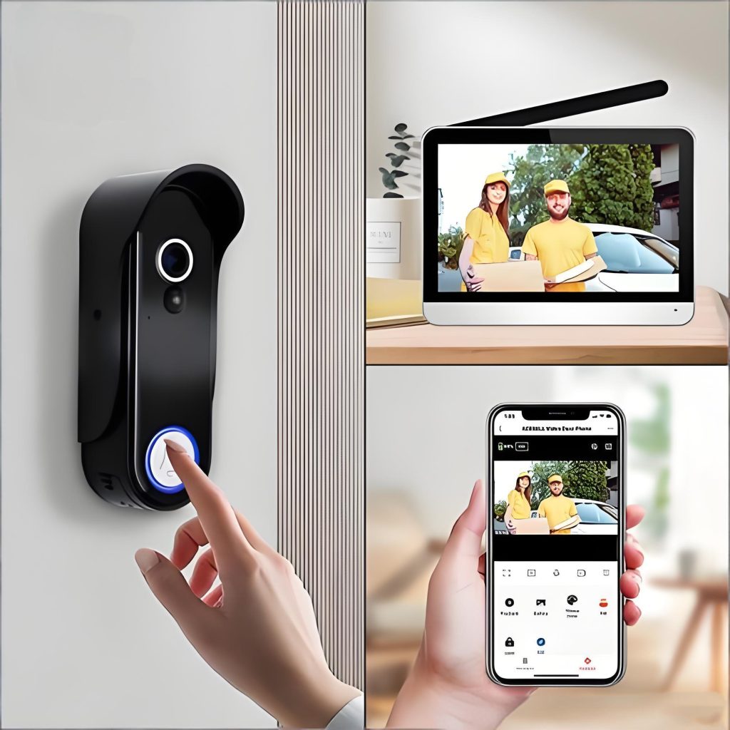
Печатные платы беспроводных дверных звонков являются основными компонентами бытовой электроники и устройств «умного дома».. Спрос на рынке продолжает расти. По мере ускорения внедрения умного дома, потребность в качественном, Высоконадежные печатные платы для беспроводных дверных звонков быстро растут.
VIII. Почему стоит выбрать платы UGPCB для беспроводных дверных звонков?
✅ Материал подложки премиум-класса : Ламинат Kingboard KB6165F Tg150 с сертификатом UL 94 В-0 огнестойкость обеспечивает безопасность и надежность продукции
✅ Соответствие международным стандартам : Проектирование и производство соответствуют IPC-6012., МПК-А-600, МПК-2221, и другие международные спецификации
✅ Экологически чистый бессвинцовый процесс : Бессвинцовая поверхность HASL соответствует экологическим требованиям RoHS.
✅ Возможности точного производства : Минимальная апертура 0,332 мм, ширина дорожки/интервал 0,42/0,46 мм для высокоточной фрезерования.
✅ Профессиональная поддержка радиочастотного проектирования : 50Управление импедансом и другая профессиональная поддержка проектирования для беспроводных дверных звонков на частоте 433 МГц.
✅ Быстрая доставка : Прототипы за 4–5 дней, доступны ускоренные варианты
IX. Руководство по запросам и заказу
UGPCB стремится предоставлять высококачественные печатные платы для беспроводных дверных звонков и печатная плата услуги «под ключ» для клиентов по всему миру. Являетесь ли вы инженером по аппаратному обеспечению, разрабатывающим новый продукт для беспроводного дверного звонка, или менеджером по закупкам, ищущим надежного поставщика печатных плат., УГКПБ — ваш надежный партнер.
Запросите ценовое предложение сегодня, чтобы получить эксклюзивные цены и специальную техническую поддержку..
📧Электронная почта : info@ugpcb.com
🌐Веб-сайт : www.ugpcb.com
Пожалуйста, предоставьте файлы дизайна печатной платы (Гербер-файлы), Билл материалов (спецификация), и любые особые требования к процессу. Профессиональная команда УГКПБ ответит в течение 24 часов с оптимизированным решением для печатных плат/PCBA.
Декларация источника данных
Технические данные, приведенные в этом документе, получены от следующих авторитетных организаций и стандартов.:
- Kingboard Laminates Holdings Limited : KB-6165F Технический паспорт ламината с медным покрытием
- IPC — Ассоциация, объединяющая электронную промышленность : МПК-6012 Квалификационные и эксплуатационные характеристики жестких печатных плат
- IPC — Ассоциация, объединяющая электронную промышленность : МПК-А-600 Приемлемость печатных плат
- IPC — Ассоциация, объединяющая электронную промышленность : МПК-2221 Общий стандарт проектирования печатных плат
- IPC — Ассоциация, объединяющая электронную промышленность : ИПК-ТМ-650 Руководство по методам испытаний (2.4.4, 2.4.8, 2.4.13.1, 2.4.24, 2.4.24.1, 2.4.24.6, 2.4.25, 2.5.5.2, 2.6.2.1)
- UL — Лаборатории страховщиков : UL 796 Стандарт для печатных монтажных плат
- UL — Лаборатории страховщиков : UL 94 Стандарт на испытания на воспламеняемость пластмассовых материалов для деталей устройств и приборов













