

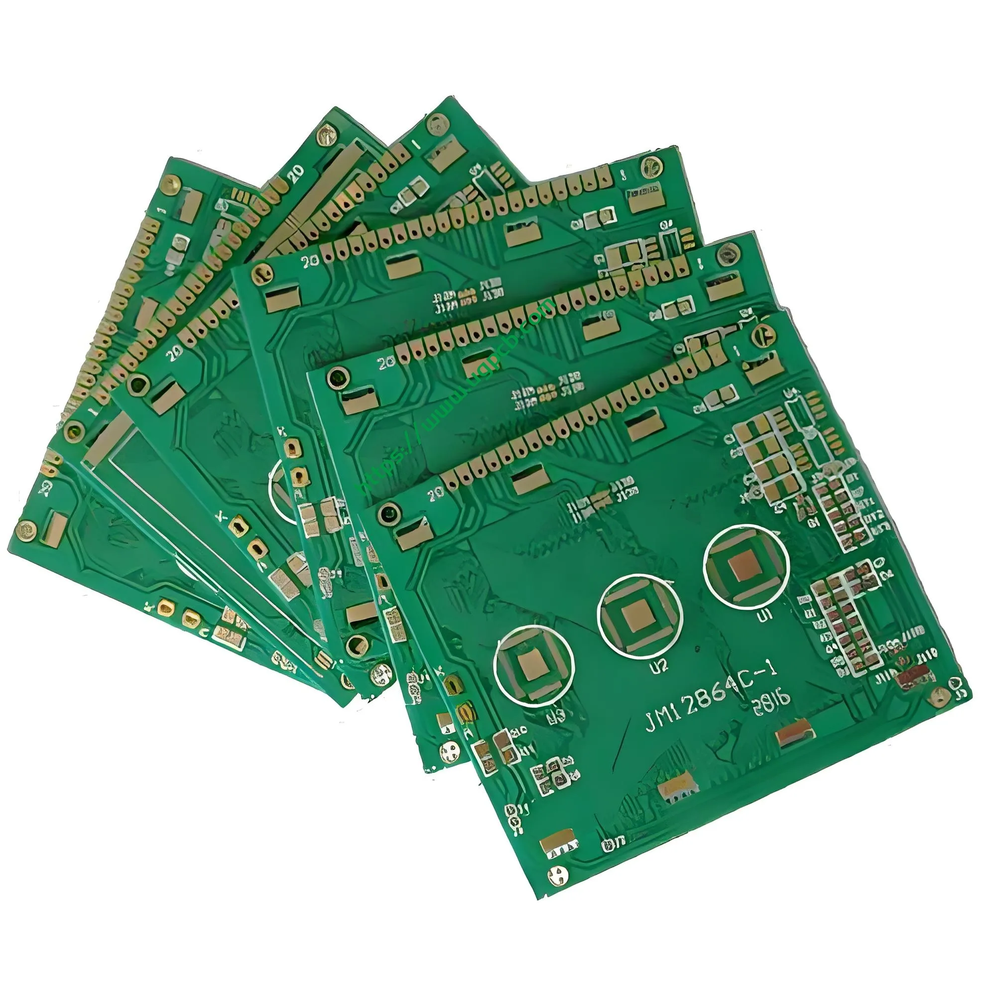
Обзор продукта: Высоконадежное решение на печатной плате для управления ЖК-дисплеем
УГКПБ представляетПечатная плата жидкокристаллического дисплея с ЖК-дисплеем (Модель: УГКПБ-ЖК-001), Высокопроизводительность2-многослойная жесткая печатная плата FR-4 разработан специально для управления жидкокристаллическими дисплеями. В качестве основного материала в этом продукте используется высококачественный ламинат Kingboard KB6165F с медным покрытием., с толщиной доски 1.6 мм и 1 унция медной фольги (примерно 35 мкм). В отделке поверхности используетсяСОГЛАШАТЬСЯ (Электролетический никель/погружение золота) процесс в 2U” . Правление измеряет 147.2 × 65 мм, с минимальным диаметром отверстия 0.22 мм и минимальная ширина линии/интервал 0.3 мм/0,27 мм.
ЭтотПлата ЖК-дисплея служит носителем критической схемы, соединяющей микросхемы драйверов дисплея с жидкокристаллическими стеклянными панелями.. Он находит широкое применение в модулях ЖК-дисплеев малого и среднего размера., дисплеи промышленных панелей управления, дисплеи автомобильной информационно-развлекательной системы, и интерфейсы человеко-машинного взаимодействия умного дома.
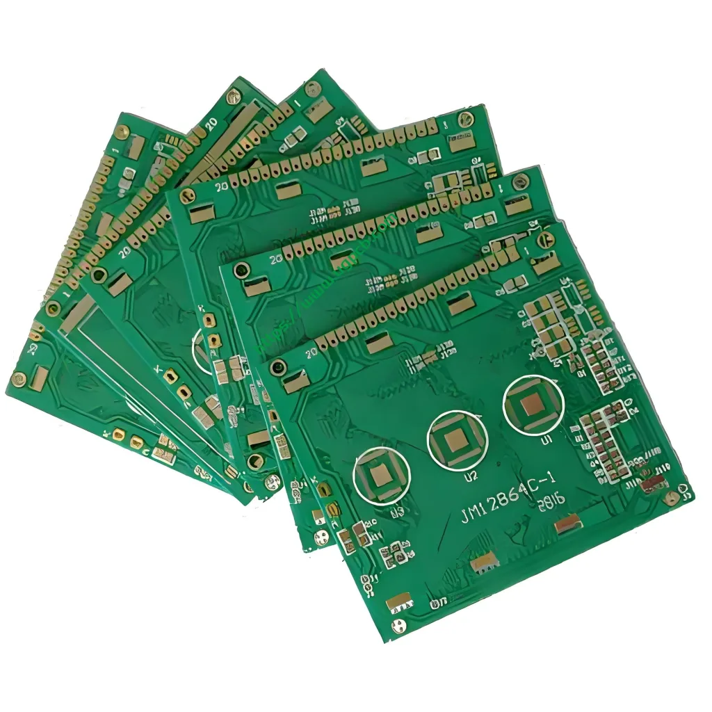
Определение продукта: Что такое печатная плата жидкокристаллического ЖК-дисплея?
Ан Плата ЖК-дисплея с жидкокристаллическим дисплеем (Печатная плата) это специализированная печатная плата, предназначенная для систем управления жидкокристаллическими дисплеями.. Он выполняет три основные функции: передача сигнала движения, Распределение энергии, и маршрутизация сигналов управления синхронизацией. В отличие от стандартного Печатные платы, анонца Плата ЖК-дисплея требует более жестких допусков по точности ширины линии, контроль импеданса, и плоскостность поверхности.
Этот продукт относится кжесткая двусторонняя печатная плата категория с 2 слои (2л). Он использует огнестойкий материал класса FR-4. (UL 94 В-0 рейтинг) и поддерживает как SMT (Технология поверхностного крепления) и процессы гибридной сборки сквозных компонентов. Плата соответствует классу IPC-6012. 2 Требования к производительности, что делает его пригодным для применения в промышленной электронике и бытовой электронике..
Технические характеристики конструкции: Критические параметры для проектирования печатных плат ЖК-дисплеев
Материал подложки: Преимущество KB6165F
В этом продукте используется ламинат Kingboard KB6165F с медным покрытием., который обеспечивает следующие ключевые характеристики производительности:
- Температура стеклянного перехода (Тг): ≥150°С, обеспечение стабильности размеров во время процессов бессвинцовой пайки оплавлением
- Температура термического разложения (Тд): 325°С, обеспечивающая превосходную термическую надежность
- Рейтинг воспламеняемости: UL 94 В-0, с самозатухающим пламенем внутри 10 секунды при испытаниях на вертикальное горение
- КТР (Коэффициент термического расширения): 12–15 ppm/°C в направлении X-Y, 40–230 ppm/°C в направлении Z, обеспечивает хорошее тепловое согласование с микросхемами драйвера ЖК-дисплея
- Каф (Проводящая анодная нить) Сопротивление: Отличные характеристики защиты от CAF, обеспечивающие долгосрочную надежность
- Совместимость без свинца: Соответствует экологическим требованиям RoHS
Согласно стандартам проектирования IPC-2221., материалы с Tg ≥150°C подходят для процессов сборки без использования свинца., способен сохранять структурную целостность при пиковых температурах пайки оплавлением, достигающих 245–260 ° C..
Подсчет слоев и дизайн стека
Особенности продукта 2 слои (2л) со стандартом 1.6 мм толщина доски. Для МПК-2221, 1.6 мм представляет собой наиболее часто используемую толщину жестких печатные платы, баланс между механической прочностью и удобством сборки.
Ширина линии и дизайн интервала
Минимальная ширина линии 0.3 мм и минимальный межстрочный интервал 0.27 мм – это тщательно подобранные параметры дляПлата драйвера ЖК-дисплея целостность сигнала. По стандартам IPC-2221, минимальные требования к расстоянию для обычного напряжения (≤30 В) следы цифровых сигналов 0.1 мм (4 мил). Этот продукт 0.27 мм (примерно 10.6 мил) расстояние намного превышает минимальные требования IPC, обеспечение достаточного запаса по качеству сигнала.
Справочник по расчету конструкции (на основе упрощенной формулы токовой нагрузки проводника внешнего слоя IPC-2221):
Допустимая токовая нагрузка внешнего слоя ≈ k × ΔT^0,448 × W^0,725 × T^0,725
где к = 0.048 (для внешнего слоя). При повышении температуры на 10°С, а 0.3 мм след с 1 Толщина меди в унцию обеспечивает теоретическую допустимую нагрузку по току примерно 1,2–1,5 А, что достаточно для требований к питанию и трассировке сигналов обычных плат драйверов ЖК-дисплея..
Минимальный диаметр отверстия
Минимальный диаметр отверстия 0.22 мм (примерно 8.7 мил) относится к категории прецизионного сверления. Под МПК-6012, стандартный допуск на диаметр просверленного отверстия составляет ±0,08 мм. (примерно ±3 мил) . Для 0.22 микроотверстия мм, производственные допуски обычно контролируются в пределах ±0,05 мм..
Поверхностная отделка: СОГЛАСЕН, что 2U”
TheСОГЛАШАТЬСЯ (Электролетический никель/погружение золота) обработка поверхности с высотой 2U” толщина золота (примерно 0.05 мкм) соответствует требованиям IPC-4552. IPC-4552 Версия А (выпущено в 2017) определяет толщину залежи золота 0.04 мкм до 0.10 мкм (1.6 мкин до 4.0 мин) и толщина никеля 3 мкм до 6 мкм.
Преимущества отделки поверхности ENIG:
- Отличная паяемость, поддержка нескольких циклов оплавления.
- Сильная возможность соединения проводов
- Превосходная стойкость к окислению и коррозии
- Плоская поверхность, подходящая для монтажа компонентов с малым шагом.
- Увеличенный срок хранения
Принцип работы: Механизмы передачи сигналов печатной платы ЖК-дисплея
TheПлата ЖК-дисплея с жидкокристаллическим дисплеем выполняет две основные функции: передача сигнала иРаспределение энергии.
1. Передача сигнала драйвера дисплея: Отображение данных с основного чипа контроллера (MCU/SoC) путешествует черезПечатная плата через микрополосковые или полосковые дорожки к микросхеме драйвера ЖК-дисплея. Микросхема драйвера преобразует цифровые сигналы в аналоговые напряжения в оттенках серого., которые затем выводятся черезпечатная платамелкие следы от электродов ITO на панели из жидкокристаллического стекла, управление углом поворота молекул жидких кристаллов для создания отображаемого изображения.
2. Маршрутизация сигнала управления синхронизацией: TheПлата ЖК-дисплея передает критические сигналы синхронизации, включая VSYNC (Вертикальная синхронизация), HSYNC (Горизонтальная синхронизация), ДКЛК (Пиксельные часы), и DE (Включение данных). Задержка передачи и согласование импеданса этих сигналов напрямую влияют на качество изображения..
3. Распределение управления питанием: TheЖК-плата преобразует входную мощность (обычно 3.3 В или 5 В) через схемы преобразования постоянного тока в постоянный для генерации нескольких уровней напряжения, необходимых для ЖК-панели., включая ВГХ (напряжение включения, обычно +15 В до +30 В), См. (напряжение затвора, обычно от −5 В до −15 В), и АВДД (аналоговое напряжение питания).
Классификация продуктов: Категории печатных плат ЖК-дисплея
Платы ЖК-дисплеев с жидкокристаллическими дисплеями можно классифицировать по следующим параметрам:
По количеству слоев
- Односторонние доски: Используется для простых ЖК-дисплеев с сегментным кодом.
- Двусторонние доски (2л): Категория этого продукта, используется для драйверов TFT-LCD дисплеев малого и среднего размера
- Многослойные платы (4L и выше): Используется для высокого разрешения., крупноформатные дисплейные модули
По отделке поверхности
- платы ЭНИГ: Категория этого продукта, предлагая лучшую общую производительность
- Платы OSP: Более низкая стоимость, подходит для бытовой электроники с коротким жизненным циклом
- HASL-платы: Подходит для плат драйверов ЖК-дисплея с более широким шагом контактов.
По приложению
- ЖК-платы для бытовой электроники: Дополнительные дисплеи смартфона, дисплеи умных часов, экраны электронных книг
- Промышленные платы управления ЖК-дисплеями: Промышленный ЧМИ, дисплеи на приборной панели, Драйверы дисплея панели управления ЧПУ
- Автомобильные ЖК-платы: Автомобильные информационно-развлекательные системы, цифровые комбинации приборов, Платы управления дисплеем HUD
- Печатные платы ЖК-дисплеев для медицинского оборудования: Мониторы пациента, ультразвуковое диагностическое оборудование, Платы драйверов дисплея системы медицинской визуализации
Основные характеристики производительности
| Параметр | Спецификация | Справочный стандарт |
|---|---|---|
| Ламинат Материал | КБ6165F (Кингборд) | - |
| Тип ламината | FR-4 Ламинат из стеклоткани, плакированный медью | UL 94 В-0 |
| Количество слоев | 2 слои (2л) | - |
| Толщина доски | 1.6 мм | МПК-2221 |
| Толщина меди внешнего слоя | 1 унция (35 мкм) | МПК-6012 Класс 2 |
| Поверхностная отделка | ТОЛЬКО 2U” (0.05 мкм Au) | МПК-4552 |
| Толщина слоя никеля | 3–6 мкм (нижний слой) | IPC-4552 Ред. А |
| Минимальный диаметр отверстия | 0.22 мм | МПК-6012 |
| Минимальная ширина линии | 0.3 мм | МПК-2221 |
| Минимальный межстрочный интервал | 0.27 мм | МПК-2221 |
| Размеры платы | 147.2 × 65 мм | - |
| Тг (Температура стеклянного перехода) | ≥150°С | - |
| Тд (Температура термического разложения) | 325°С | - |
| КТР (Направление X-Y) | 12–15 частей на миллион/°C | - |
| Рейтинг воспламеняемости | UL 94 В-0 | УЛ 94 |
| Дуговое сопротивление | ≥60 секунд | - |
| Поверхностное удельное сопротивление | ≥2,6 × 10⁸ МОм | - |
| Объемный удельное сопротивление | ≥3,4 × 10⁹ МОм·см | - |
Анализ структуры продукта
TheПлата ЖК-дисплея с жидкокристаллическим дисплеем структура состоит из следующих слоев снаружи внутрь:
1. Внешний слой – обработка поверхности ENIG: Золотой слой на высоте 2U” (примерно 0.05 мкм) защищает нижележащий слой никеля от окисления. Нижний слой никеля толщиной 3–6 мкм служит диффузионным барьером между медью и золотом..
2. Слой медной фольги: 1 унция (примерно 35 мкм) электроосажденная медная фольга, выгравирован для формирования схемы.
3. Диэлектрический слой: Стеклоткань марки ФР-4, пропитанная эпоксидной смолой., примерно 0.7 толщина мм (один слой), обеспечение электрической изоляции и механической поддержки.
4. Слой медной фольги: Нижний слой 1 унция меди, образующая рисунок нижней цепи.
5. Внешний слой – обработка поверхности ENIG: Симметричная обработка ENIG, соответствующая верхнему слою.
Особенности продукта: Почему стоит выбрать печатную плату с ЖК-дисплеем UGPCB?
① Высокоточное производство: Минимальный диаметр отверстия 0.22 мм и минимальная ширина линии/интервал 0.3 мм/0,27 мм соответствуют требованиям к прокладке плат драйверов ЖК-дисплеев высокой плотности..
② Премиум-материалы для подложек: Kingboard KB6165F высококачественный материал FR-4 с Tg ≥150°C и UL 94 В-0 Класс воспламеняемости обеспечивает совместимость с бессвинцовыми процессами и долгосрочную надежность..
③ Стандартизированная обработка поверхности: ТОЛЬКО 2U” процесс соответствует IPC-4552, обеспечение превосходной паяемости, стойкость к окислению, и увеличенный срок хранения.
④ Строгий контроль качества: Продукция проходит полный технологический контроль качества по классу IPC-6012. 2 стандарты, допуск диаметра закрывающего отверстия (±0,08 мм), Толщина отверстия в меди (≥20 мкм), целостность паяльной маски, и электрические испытания.
⑤ Дизайн, оптимизированный для ЖК-дисплея: Контроль импеданса, целостность сигнала, и целостность питания оптимизированы специально для приложений управления жидкокристаллическими дисплеями.
Производственный процесс: От сырья к готовому продукту
UGPCB следует строгому стандартному производственному процессу дляПлаты ЖК-дисплея:
1. Материальная резка →2. Перенос рисунка внутреннего слоя (позиционирование сверла и регистрационные метки) →3. Бурение (минимальный диаметр отверстия 0.22 мм ± 0.08 мм) →4. Химическое осаждение меди/гальваника (металлизация отверстий, толщина отверстия меди ≥20 мкм) →5. Перенос рисунка внешнего слоя (ширина линии 0.3 мм / расстояние 0.27 мм) →6. Узорное покрытие (наращивание меди до 1 унция) →7. Офорт →8. Печать паяльной маски →9. ЭНИГ Поверхностная обработка (СОГЛАШАТЬСЯ, толщина золота 2U”) →10. Профилирование (размеры 147.2 × 65 мм) →11. Электрические испытания (100% электрические испытания) →12. Заключительная проверка (АОИ + Визуальный осмотр) →13. Упаковка и доставка
Типичные сценарии применения
📱 Бытовая электроника: Дополнительные дисплеи смартфона, дисплеи умных часов, Печатные платы драйверов экрана электронной книги.
🏭 Производственный контроль: Человеко-машинные интерфейсы ПЛК (ЧМИ), дисплеи промышленных приборов, Платы драйвера дисплея панели управления ЧПУ.
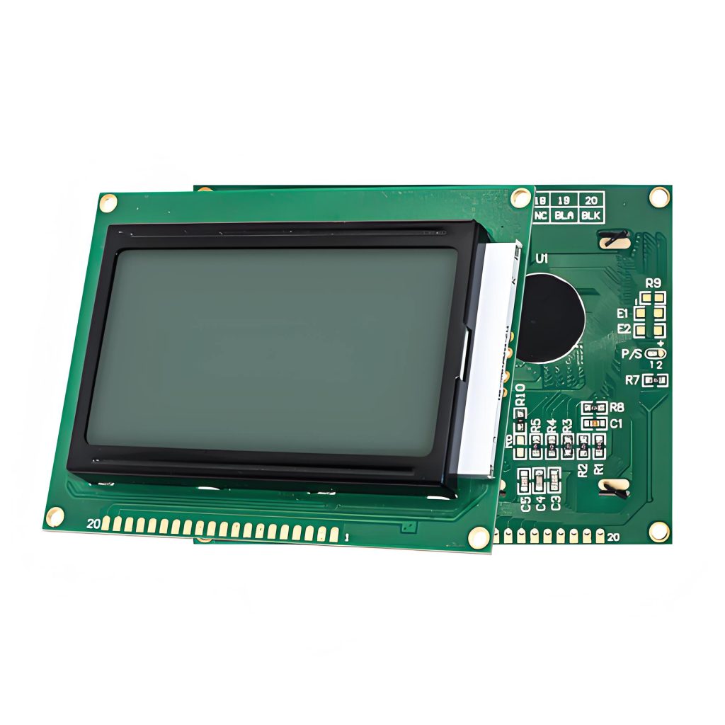
🚗 Автомобильная электроника: Автомобильные информационно-развлекательные системы, цифровые комбинации приборов, проекционный дисплей (HUD) платы управления дисплеем.
🏥Медицинское оборудование: Мониторы пациента, ультразвуковое диагностическое оборудование, Печатные платы драйвера дисплея системы медицинской визуализации.
🏠 Умный дом: Дисплеи интеллектуальной системы контроля доступа, умные панели управления бытовой техникой, Печатные платы модуля дисплея системы внутренней связи.
Почему выбирают UGPCB?
UGPCB приносит годы Плата ЖК-дисплея производственный опыт для каждого проекта. Мы используем сырье премиум-класса, такое как Kingboard KB6165F., строго соблюдать класс IPC-6012 2 стандарты качества, и эксплуатировать высокоточное оборудование для сверления и построения контуров.. Нужен ли вам ЖК-дисплей Прототипирование печатной платы или серийное производство, UGPCB обеспечивает высокую точность, высоконадежные продуктовые решения.
📞 Получите решение для печатной платы ЖК-дисплея сегодня
UGPCB Платы ЖК-дисплеев с жидкокристаллическими дисплеями успешно применяются во многих промышленных, автомобильный, и проекты дисплеев бытовой электроники. Нужен ли вам Прототипирование печатной платы ЖК-дисплея для проверки проекта или печатная плата услуги сборки под ключ, UGPCB обеспечивает полную поддержку процесса от изготовления печатных плат до печатная плата SMT Assembly.
Свяжитесь с профессиональной командой UGPCB сегодня, чтобы получить индивидуальное решение для печатной платы с ЖК-дисплеем!
📧 Электронная почта: [info@ugpcb.com]
📞 Телефон: [+86-755-ХХХХХХХ]
🌐 Сайт: [www.ugpcb.com]
Атрибуция источника данных
Технические стандарты и данные, приведенные в этом документе, взяты из следующих авторитетных источников.:
- МПК-6012 –Квалификационные и эксплуатационные характеристики жестких печатных плат – Определяет допуски на диаметр отверстий печатной платы. (стандарт ±0,08 мм), Толщина отверстия в меди (Сорт 2 ≥20 мкм), и требования к классу производительности
- МПК-2221 –Общий стандарт проектирования печатных плат – Определяет требования к ширине/расстоянию линий и формулы расчета допустимой нагрузки по току.
- IPC-4552 Версия А (изданный 2017) –Технические характеристики для химического никеля/иммерсионного золота (СОГЛАШАТЬСЯ) Покрытие печатных плат – Определяет требования ENIG к толщине покрытия: никель 3–6 мкм, золото 0,04–0,10 мкм
- UL 94 –Стандарт на безопасность воспламеняемости пластмассовых материалов для деталей устройств и приборов – В-0 рейтинг требует самозатухания пламени в течение 10 секунды
- Техническое описание продукта Kingboard KB6165F – Технические параметры подложки (Тс ≥150°С, Тд 325°С, UL 94 В-0, и т. д.)
- ГБ/Т 4677 –Методы испытаний печатных плат – Используется вместе со стандартами IPC в качестве эталонов для проверок.













