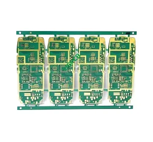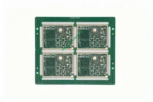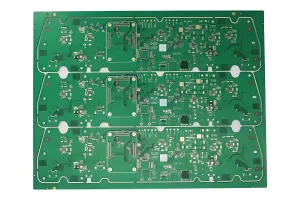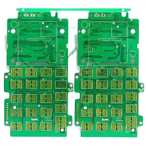
1. Produktübersicht
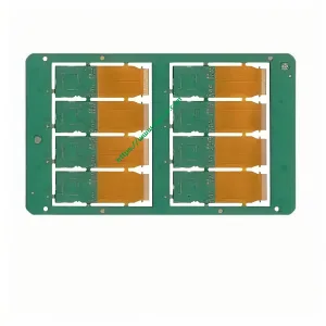
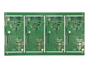
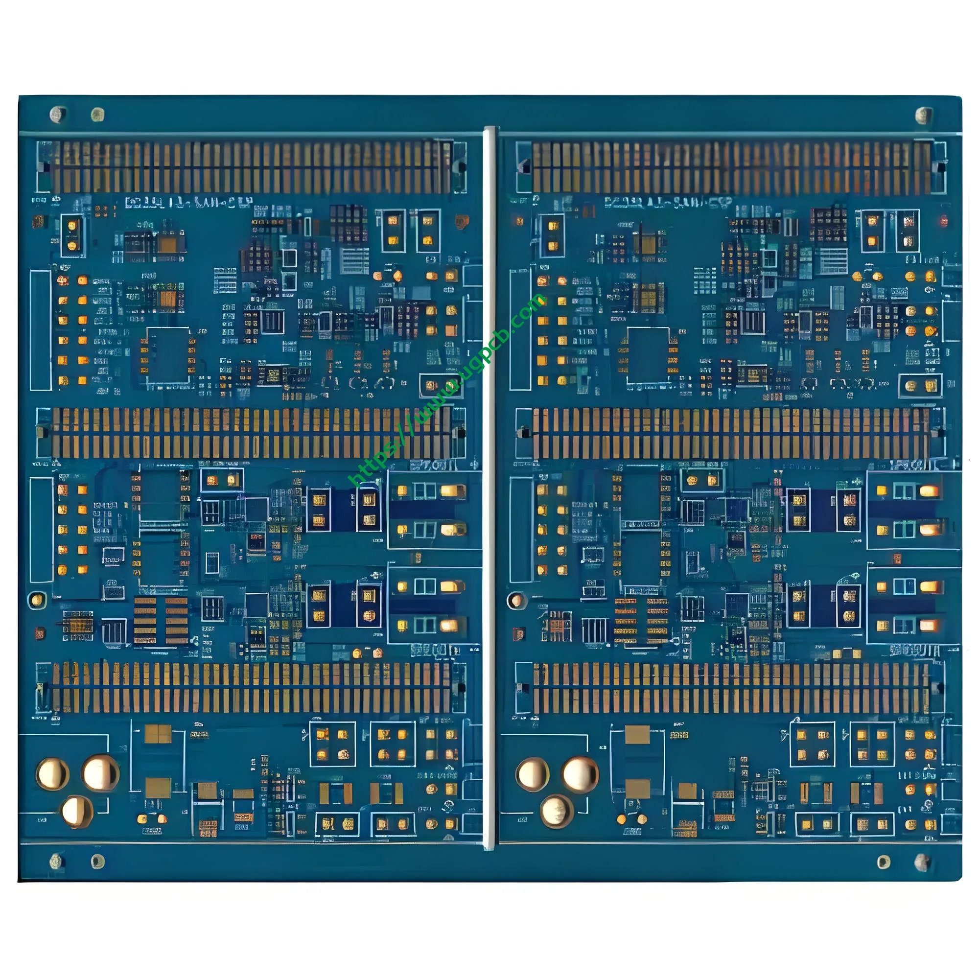
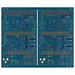
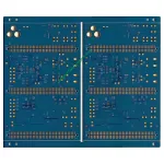
Im Bereich von hochdichte Verbindung (HDI) Leiterplatten, Die12-layer 2+N+2 board represents an important direction in advanced PCB manufacturing technology. UGPCB12-layer 2+N+2 HDI board uses ISOLA high-performance substrate material, with a finished board thickness of 2.0 mm, 1 oz copper on both outer and inner layers, a minimum via diameter of 0.1 mm, line width/spacing of 0.1 mm, BGA pad diameter of 0.15 mm, and electroless nickel/immersion gold (ZUSTIMMEN) Oberflächenbeschaffung.
Das12-Schicht Leiterplatte is a typical high-density interconnect Mehrschichtplatine suitable for electronic products with demanding requirements for signal integrity, routing density, und Zuverlässigkeit. Als2+N+2 structure HDI -Vorstand, it features two buildup layers on each side, with N core layers in the middle, supporting stacked or staggered microvia structures.

2. Produktdefinition
2.1 What Is a 2+N+2 HDI Board?
A2+N+2 HDI-Board is a high-density interconnect printed circuit board manufactured using a sequential lamination process. Der “2” in its name represents two buildup layers on each side, während “N” represents the number of core layers in the middle. For this product, the total layer count is 12, meaning a 2+8+2 structure — two buildup layers on each side and eight core layers in the middle.
DasHDI PCB belongs to Type III (as defined by IPC-2226), a commonly used HDI stackup solution supporting medium pin-count, Hochdichte BGA Komponente Routenführung. Der2+N+2 PCB stackup design significantly improves routing density, supports successful routing of ultra-fine-pitch BGAs with pitches as small as 0.4 mm, reduces overall layer count, and minimizes signal attenuation.
2.2 Applicable International Standards
Das Design, Herstellung, and acceptance of this product strictly comply with the following IPC international standards:
- IPC-6012F - -Qualifikations- und Leistungsspezifikation für starre Leiterplatten: This is the internationally recognized performance specification for rigid printed circuit boards, covering the entire process from material selection to finished product, including quality indicators, qualification, and performance requirements for each process step.
- IPC-2221C - -Allgemeiner Standard für Leiterplattendesign: This is the foundation design standard for all documents in the IPC-2220 series, establishing generic requirements for printed board design.
- IPC-4101E - -Spezifikation für Basismaterialien für starre und mehrschichtige Leiterplatten: This specification covers requirements for base materials (laminate or prepreg) used primarily for rigid or multilayer printed boards.
3. Entwurfsrichtlinien
3.1 2+N+2 Stackup Structure Design
Der12-layer 2+N+2 PCB stackup design follows the core design principles for HDI boards:
- Priority on ground planes: Ground planes are prioritized because they transmit signals in microstrip configurations.
- Low impedance and low noise: A ground-plane-based 12-layer PCB-Design achieves low ground impedance and low noise.
- High-speed signal routing: Intermediate layers between planes are used for high-speed signal traces, with tight coupling between signal layers.
- Adjacent plane and signal layers: Plane layers and signal layers should be placed on adjacent layers.
- Tight plane coupling: Large-area power and ground planes should be tightly coupled together.
3.2 Signalintegritätsdesign
Gemäß IPC-2221C, impedance tolerance and conductor layer isolation areas are critical considerations in Hochgeschwindigkeits-PCB-Design. Für die12-layer 2+N+2 HDI board, special attention should be paid to:
- Impedanzkontrolle: Mit 1 Oz Kupfer (etwa 35 μm) on both outer and inner layers, precise line width/spacing control is required to achieve target impedance.
- Microvia structure: Der 0.1 mm minimum via diameter falls within the microvia category (≤ 0.15 mm as defined by IPC-2221 and IPC-6012).
- BGA breakout: Der 0.15 mm BGA pad combined with 0.1 mm line width/spacing supports successful breakout for 0.4 mm pitch BGAs.
4. Funktionsprinzipien
Der12-layer 2+N+2 HDI board operates based on the interconnection and signal transmission of multiple conductive layers. Its core operating mechanisms include:
4.1 Signal Transmission Paths
HDI boards achieve interlayer electrical connections through the following via types:
- Blind Vias: Connect from an outer layer to a specific inner layer without penetrating the entire board thickness.
- Vergrabene Durchkontaktierungen: Exist only between inner layers.
- Stacked microvias: Multiple microvias stacked vertically to form a path through multiple buildup layers.
4.2 Power Distribution and Grounding
The power distribution network (PDN) der12-Schichtplatine is optimized through:
- Large-area power planes tightly coupled with ground planes, forming effective decoupling capacitance.
- Ground layers serving as return paths for signals, reducing loop inductance.
- Signal layers tightly coupled with adjacent plane layers, reducing electromagnetic interference (EMI).
5. Primäre Anwendungen und Anwendungsfälle
5.1 Target Application Areas
Der12-layer 2+N+2 HDI board, with its high-density interconnect capability and excellent electrical performance, is primarily used in the following areas:
| Anwendungsbereich | Typical Products | Hauptanforderungen |
|---|---|---|
| 5G Infrastruktur | 5G Basisstationen, AAU, RRU | High frequency, hohe Geschwindigkeit, geringer Verlust |
| Rechenzentren | Server, Schalter, Speichergeräte | High-speed data transmission, hohe Zuverlässigkeit |
| Hochleistungs-Computing | KI-Beschleunigerkarten, HPC | High-density BGA, Signalintegrität |
| Wired/Wireless Communications | Optical modules, Router, microwave equipment | High-frequency performance, low insertion loss |
| Kfz -Elektronik | Adas, Automobilradar (77 GHz) | Hohe Zuverlässigkeit, temperature resistance |
| Luft- und Raumfahrt und Verteidigung | Avionik, Radarsysteme | Extreme environment reliability |
ISOLA materials such as TerraGreen® 400G are specifically suited for next-generation 5G infrastructure, data center systems, Hochleistungsrechnen, wired/wireless communications, and AI applications, supporting extremely high data transmission rates exceeding 100 Gb/s.

5.2 Compatible Product Types
- High-end smartphone mainboards
- Communication base station RF boards
- High-performance server backplanes
- AI training/inference accelerator cards
- High-speed optical modules
- Automotive radar sensor boards
6. Produktklassifizierung
Based on standard PCB industry classification methods, Dieses Produkt kann wissenschaftlich wie folgt kategorisiert werden:
6.1 By Product Structure
Rigid board — Manufactured using rigid substrate materials (FR4/ISOLA).
6.2 Für Schichtzahl
Mehrschichtplatte — Featuring 12 leitfähige Schichten, bonded by insulating dielectric materials and interconnected through vias.
6.3 By Manufacturing Process
HDI -Vorstand (Verbindungsplatine mit hoher Dichte) — Featuring a 2+N+2 sequential lamination structure, classified as a second-order HDI board (2+C+2).
6.4 By IPC-2226 Stackup Type
Type III stackup — 2+N+2 or higher-order stacked/staggered microvia structures.
6.5 By IPC-6012 Quality Class
Available to meetKlasse 2 (dedicated-service electronic products) oderKlasse 3 (Elektronische Produkte mit hoher Zuverlässigkeit) requirements as per customer specifications.
7. Materialien verwendet
7.1 Substrat: ISOLA Series Materials
This product uses ISOLA high-performance copper-clad laminates. ISOLA is a leading material supplier in the high-frequency, high-speed PCB sector, with its products widely used in high-speed digital, high-frequency analog, RF/microwave, and other advanced circuit designs.
Typical properties of ISOLA materials (TerraGreen® 400G as an example):
| Eigentum | Typischer Wert | Testmethode |
|---|---|---|
| Glasübergangstemperatur (Tg DSC) | 200°C | IPC-TM-650 2.4.25C |
| Glasübergangstemperatur (Tg DMA) | 215°C | IPC-TM-650 2.4.24.4 |
| Zersetzungstemperatur (Td @5% weight loss) | >380°C | IPC-TM-650 2.4.24.6 |
| Dielektrizitätskonstante (Dk) | 3.15 | IPC-TM-650 2.5.5.5 |
| Dissipationsfaktor (Df) | 0.0017 | IPC-TM-650 2.5.5.5 |
| UL-Entflammbarkeitsklasse | UL 94 V-0 | UL File E41625 |
ISOLA materials comply with IPC-4101/134 and offer the following advantages:
- Halogen-free and RoHS compliant
- Ausgezeichnetes CAF (conductive anodic filament) Widerstand
- Niedrige Feuchtigkeitsabsorption
- Withstands up to 6 reflow cycles at 260°C
- FR-4 process compatible — can be processed using standard PCB-Ausrüstung
7.2 Kupferfolie
- Inner and outer layer copper thickness: 1 oz (etwa 35 μm)
- Copper foil type: HVLP3 (ultra-low profile) or RTF (rückwärts behandelt) copper foil available upon request
7.3 Brettdicke
- Dicke der fertigen Platte: 2.0 mm
8. Leistungsspezifikationen
8.1 Key Electrical Specifications
| Parameter | Spezifikation | Notizen |
|---|---|---|
| Schichtzahl | 12 Schichten | 2+N+2 structure |
| Dicke der fertigen Platte | 2.0 mm | - |
| Kupferdicke der äußeren Schicht | 1 oz (35 μm) | Fertiges Kupfer |
| Kupferdicke der inneren Schicht | 1 oz (35 μm) | - |
| Minimaler Via-Durchmesser | 0.1 mm | Laser-drilled microvia |
| Mindestlinienbreite | 0.1 mm | - |
| Mindestzeilenabstand | 0.1 mm | - |
| BGA Pad Diameter | 0.15 mm | Unterstützung 0.4 mm pitch BGA |
| Oberflächenbeschaffung | ZUSTIMMEN (Elektrololes Nickel/Immersion Gold) | IPC-4552 compliant |
8.2 Reliability Performance
Gemäß IPC-6012F, rigid printed boards must meet the following reliability requirements:
- Electrical performance: Isolationsresistenz, dielectric withstanding voltage, Impedanzkontrolle, usw.
- Mechanical performance: Schälfestigkeit, Verzug, Dimensionsstabilität, usw.
- Environmental performance: Thermalradfahren, Feuchtigkeitsprüfung, salt spray testing, usw.
IPC-6012F has introduced several new requirements for microvia structure reliability, including copper wrap plating, intermediate target lands, microsection evaluation, inner layer plating, and dielectric spacing and reliability issues for microvia structures.
IPC-6012F has increased the minimum copper thickness requirement for plated-through hole barrel walls — raised to 28 μm for Class 3/A (previously 25 μm).
8.3 Wärmeleistung
ISOLA materials with Tg ≥ 200°C and Td > 380°C support lead-free soldering processes and multiple reflow cycles.
9. Produktstruktur
Der2+N+2 HDI-Board via structure includes:
- Laser blind vias: From outer layers (L1/L12) to Layer 3/Layer 10 (buildup section), 0.1 mm diameter
- Laser blind vias: From Layer 3/Layer 10 to inner core layers
- Mechanical through vias: Through the core section (Schichten 4-9)
- Stacked microvias: Blind vias can be stacked vertically for multi-layer connections
10. Produktmerkmale
10.1 High-Density-Verbindungsfähigkeit
- 0.1 MM Microvias: Support ultra-high-density routing
- 0.1 mm line width/spacing: Enable fine-line design
- 0.15 mm BGA pads: Unterstützung 0.4 mm pitch ultra-fine-pitch BGAs
10.2 Hervorragende Signalintegrität
- ISOLA low-loss material (Df so niedrig wie 0.0017) ensures low high-frequency signal attenuation
- 2+N+2 structure supports precise impedance control
- Ground planes tightly coupled with signal layers reduce EMI
10.3 Hohe Zuverlässigkeit
- Complies with IPC-6012F Class 2/Class 3 Anforderungen
- ISOLA material with Tg ≥ 200°C and Td > 380°C
- ENIG surface finish provides excellent solderability and oxidation resistance
10.4 Prozesskompatibilität
- ISOLA materials are compatible with standard FR-4 process flows
- Unterstützt sequentielles Laminieren
- Allows multiple reflow cycles
11. Ablauf des Herstellungsprozesses
The 12-layer 2+N+2 HDI board manufacturing process is as follows:
11.1 Core Board Manufacturing (Innere Schichten)
- Materialschneiden: Cut ISOLA substrate per MI requirements
- Bildung der inneren Schaltkreise: Apply photoresist → expose → develop → etch → strip to form inner layer circuit patterns
- Inner layer AOI: Automated optical inspection to ensure circuit quality
- Braune Oxidbehandlung: Enhance adhesion between inner layer copper and prepreg
11.2 First Lamination
- Stapeln: Stack inner layer cores with prepreg per the stackup structure
- Laminierung: Bond multiple layers into one unit under high temperature and pressure
11.3 First Drilling and Via Metallization
- Laserbohrung: Drill 0.1 MM Microvias
- Desmear: Remove carbonized residue from laser drilling
- Via metallization: Electroless copper deposition to form conductive layer on via walls
- Panel plating: Build up copper thickness on via walls
11.4 Buildup Layer (Äußere Schicht) Herstellung
- Bildung von Schaltkreisen der äußeren Schicht: Repeat inner layer circuit formation process
- Outer layer AOI: Automatisierte optische Inspektion
11.5 Second Lamination (falls erforderlich)
- Secondary lamination: Multiple sequential lamination steps may be required for 2+N+2 structures
11.6 Final Finishing
- Outer layer drilling: Mechanical through-hole drilling
- Via metallization and plating: Through-hole metallization and copper build-up plating
- Outer layer circuits: Bilden Sie Schaltkreismuster der äußeren Schicht
- Lötmaske: Apply solder mask ink
- Oberflächenbeschaffenheit: ZUSTIMMEN (Elektrololes Nickel/Immersion Gold) — electroless nickel (3–6 μm) + Eintauchen Gold (0.05–0,1 μm) für IPC-4552
- Legendendruck: Silk-screen component designators and other markings
- Profilrouting: Routenführung, V-Schnitt, usw.
- Elektrische Prüfung: Fliegende Sonde oder Vorrichtungstests
- Endkontrolle: Visual inspection and packaging
12. Vorteile der ENIG-Oberflächenbeschaffenheit
Dieses Produkt verwendetZUSTIMMEN (Elektrololes Nickel/Immersion Gold) Oberflächenbeschaffung, offering the following core advantages:
| Vorteil | Beschreibung |
|---|---|
| Hervorragende Ebenheit der Oberfläche | Ideal for fine-pitch BGA and SMT assembly |
| Superior solderability | Supports multiple reflow cycles (3+ mal) |
| Lange Haltbarkeit | 12+ months storage life |
| Strong oxidation resistance | Gold layer protects copper from oxidation |
| Gute elektrische Leitfähigkeit | Suitable for high-frequency signal transmission |
The ENIG process chemically deposits a nickel-phosphorus alloy layer (approximately 3–6 μm thickness) und eine Goldschicht (approximately 0.05–0.1 μm thickness) on the PCB copper surface.
13. Why Choose UGPCB’s 12-Layer 2+N+2 HDI Board?
- International standard compliance: Strictly follows IPC-6012F, IPC-2221C, IPC-4101E, und andere internationale Standards
- Premium-Materialsicherheit: Uses ISOLA high-performance substrate for high-frequency, high-speed performance
- Erweiterte Fertigungsmöglichkeiten: Precision processing for 0.1 mm microvias and 0.1 mm line width/spacing
- Comprehensive quality control: Full-process quality management from incoming material inspection to final product testing
- Professional engineering support: Provides DFM (Design für die Herstellung) reviews and impedance design support
14. Fordern Sie ein Angebot an
UGPCB is committed to providing high-qualityHDI PCB manufacturing services to customers worldwide. Whether you need a12-layer 2+N+2 HDI board or other layer counts and structures ofMehrschichtige PCBs, we offer professional technical support and competitive pricing.
So erhalten Sie ein Angebot:
- Submit design files: Send Gerber files, Bohrdateien, and stackup specifications to our sales team
- Specify technical requirements: Include impedance requirements, material preferences, Oberflächenbeschaffung, Menge, usw.
- Technische Überprüfung: Our engineers will perform DFM checks to ensure manufacturability
- Receive a quote: Get a competitive price and lead time quickly
Kontaktieren Sie uns
Send yourLeiterplatte design files to our sales email or submit an inquiry through our website. Our technical team will respond within 24 Std..
Erklärung zur Datenquelle
The technical data and standard information cited in this document are sourced from the following authoritative organizations:
- IPC (Verband zur Verbindung der Elektronikindustrie) — IPC-6012FQualifikations- und Leistungsspezifikation für starre Leiterplatten (September 2023); IPC-2221CAllgemeiner Standard für Leiterplattendesign (December 2023); IPC-4101ESpezifikation für Basismaterialien für starre und mehrschichtige Leiterplatten (March 2017); IPC-4552Leistungsspezifikation für chemisches Nickel/Immersionsgold (ZUSTIMMEN) Beschichtung für Leiterplatten
- Isola -Gruppe — TerraGreen® 400G Product Data Sheet
- UL (Underwriters Laboratories) – UL 94 V-0 Entflammbarkeitsbewertung, UL File Number E41625
- Fachliteratur aus der Industrie — HDI PCB stackup design and 2+N+2 structure technical documentation