
In today’s fast-paced electronics landscape, the demand for compact, 경량, and highly reliable interconnect solutions has never been greater. Whether you are developing wearable devices, medical instruments, or advanced digital systems, 리지드 플렉스 PCB are the cornerstone technology that bridges the gap between rigid stability and dynamic flexibility. ~에 UGPCB, we specialize in delivering precision-engineered rigid-flex PCB prototypes that meet the most stringent design and performance requirements. This guide will walk you through every aspect of our featured product — a 2+2+2 리지드 플렉스 PCB built with FR-4 and polyimide — and show you why it is the optimal choice for your next 디지털 PCB 프로토타입 프로젝트.
What is a Rigid-Flex PCB (R-FPCB)?
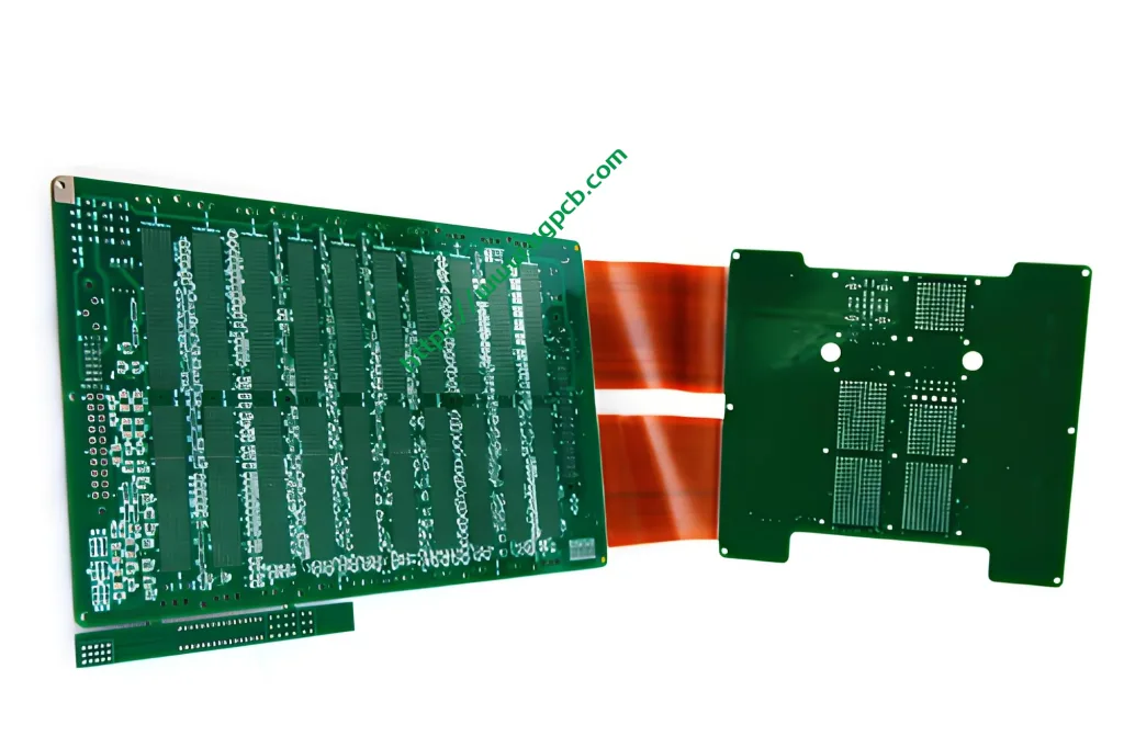
에이 리지드 플렉스 PCB, often abbreviated as R-FPCB, is a hybrid printed circuit board that combines rigid and flexible substrate materials into a single integrated structure. Unlike traditional rigid PCB that use only stiff laminates, or standalone flexible circuits, 리지드 플렉스 PCB allow for three-dimensional packaging by eliminating connectors and ribbon cables between rigid sections. This seamless integration significantly enhances signal integrity, reduces assembly costs, and improves overall device reliability. The “2+2+2” designation describes the layer stack-up: two rigid outer layers, two flexible inner layers, and two additional rigid layers bonded together, creating a 6-layer 리지드 플렉스 PCB perfectly suited for digital applications where space and weight are at a premium.
[이미지 제안: Cross-sectional diagram of a 2+2+2 rigid-flex PCB showing rigid FR-4 sections, flexible polyimide layers, and plated through-holes.
Alt text: Cross-section of 2+2+2 rigid-flex PCB stackup with FR-4 rigid layers and PI flexible layers]
제품개요: UGPCB 2+2+2 Rigid-Flex PCB 프로토타입
UGPCB에, our standard rigid-flex PCB prototype offering is engineered to accelerate your product development cycle. The key specifications of our featured build are:
-
모델: 리지드 플렉스 PCB (R-FPCB)
-
재료: FR-4 (엄격한) + PI – Polyimide (유연한)
-
레이어 구조: 2+2+2 (6-layer rigid-flex construction)
-
솔더 마스크 색상: 녹색 / 하얀색
-
완성된 두께: 1.0 mm (rigid area) + 0.15 mm (flexible area)
-
구리 두께: 0.035 mm (1 온스) on all layers
-
표면 처리: 이머젼 골드 (동의하다)
-
최소 선 너비 / Distance: 0.1 mm / 0.1 mm
-
애플리케이션: Digital rigid-flex PCB prototype fabrication
This configuration is optimized for high-density digital circuits that require both mechanical bending and rigid component mounting zones.
How a Rigid-Flex PCB Works
The operating principle of a 리지드 플렉스 PCB leverages the unique material properties of its constituents. Rigid layers, typically made from FR-4 epoxy glass laminate, provide structural support and a stable platform for surface-mount and through-hole components. Flexible layers, constructed from 폴리이미드 (PI) 영화, act as integrated “hinges” that can be dynamically bent or statically folded to fit into compact enclosures. Electrically, the layers are interconnected through plated through-holes and buried vias, forming a continuous PCB 회로. By eliminating board-to-board connectors, 그만큼 리지드 플렉스 PCB reduces signal attenuation and reflection, which is critical in high-speed digital applications. When the flexible section is bent, the polyimide substrate withstands stress far better than FR-4, provided the bend radius respects the material’s mechanical limits.
Design Essentials for 2+2+2 RIDID-FLEX PCB
Designing a 2+2+2 리지드 플렉스 PCB requires a deep understanding of mechanical and electrical constraints. Key RIDID-FLEX PCB 설계 considerations include:
-
굽힘 반경 계산: IPC-2223에 따르면, for dynamic flex applications, the minimum bend radius should be at least 10 times the flex circuit thickness. With our 0.15 mm flexible layer, the recommended minimum bend radius is 1.5 mm.
-
Trace Routing in Bend Areas: Lines and spaces must align perpendicular to the bend axis to avoid copper cracking. 우리의 0.1 mm trace/space capability allows dense routing while maintaining reliability.
-
Layer Cross-Section: The transition zone from rigid to flex must be carefully modeled to avoid stress concentrators. Bookbinder-style construction is used to progressively release the flexible layers from the rigid stack.
-
Via Placement: No plated vias should be placed within the bend zone, as they are prone to fatigue failure. Blind and buried vias in rigid sections enhance via-in-pad designs for high-density PCB.
By addressing these rigid-flex PCB design guidelines, UGPCB can transform your schematic into a robust digital rigid-flex prototype that performs flawlessly.
애플리케이션 및 사용 사례
The versatility of a 2+2+2 리지드 플렉스 PCB makes it ideal for a wide array of digital and mixed-signal systems. Common rigid-flex PCB applications 포함하다:
-
Wearable Electronics: 스마트워치, 피트니스 트래커, and medical patches where the board must conform to body contours.
-
의료 기기: Implantable diagnostics, 보청기, and endoscopic imaging systems requiring repeated sterilization cycles and high reliability.
-
Industrial IoT Sensors: Compact sensor nodes that must fit into small housings and withstand vibration.
-
항공우주 및 국방: 항공전자공학, 위성 시스템, and missile guidance electronics benefiting from weight reduction and high shock resistance.
-
Consumer Digital Products: Foldable smartphones, 카메라, and portable gaming devices relying on 리지드 플렉스 PCB technology for miniaturization.
In digital PCB 프로토 타이핑, the ability to test full system functionality with integrated flex eliminates the variables introduced by connectors, enabling faster validation of signal integrity and power distribution.
Classification of Rigid-Flex PCBs
To properly situate our product within industry standards, rigid-flex boards are classified according to IPC-6013 based on construction and intended end-use:
-
유형 1: Single-sided flexible PCB
-
유형 2: Double-sided flexible PCB with plated through-holes
-
유형 3: Multilayer flexible PCB
-
유형 4: Rigid-flex multilayer PCB – Our 2+2+2 configuration falls squarely into this category, where rigid and flexible layers are intermixed to form a single integrated circuit board.
-
유형 5: Flex or rigid-flex multilayer with rigidized stiffeners
유형 4 is the most prevalent for digital applications because it allows complex interconnects across multiple rigid domains while maintaining full PCB compatibility.
Materials and Their Performance
In a 2+2+2 리지드 플렉스 PCB, material selection directly impacts performance and longevity.
-
FR-4 (Rigid Laminate): A flame-retardant epoxy/glass composite that provides excellent dimensional stability, a dielectric constant (DK) of approximately 4.2–4.6 at 1 MHz, and a glass transition temperature (Tg) typically around 135°C to 170°C. In our build, high-Tg FR-4 is standard to withstand lead-free assembly temperatures.
-
폴리이미드 (Flexible Laminate): The polyimide film offers outstanding thermal resistance (continuous service up to 200°C), extremely low outgassing, and a Dk of around 3.5 ~에 1 MHz. Its flexibility endures millions of dynamic bend cycles when the bend radius guideline is followed.
-
이머젼 골드 (동의하다) 표면 마감: Electroless Nickel Immersion Gold provides a flat, solderable surface with a typical nickel thickness of 3–6 µm and gold thickness of 0.05–0.15 µm. It ensures excellent shelf life, wire-bonding capability, and uniform coplanarity for fine-pitch components – critical in high-density PCB 집회.
주요 기능 및 이점
UGPCB 2+2+2 rigid-flex PCB prototype offers distinct advantages tailored for the digital designer:
-
Ultra-Miniaturization: Combines six layers of interconnect in a package that can fold into a fraction of the space required by separate rigid boards and cabling.
-
탁월한 신호 무결성: Controlled impedance traces are maintained across the entire PCB without connector discontinuities. For a 0.1 mm trace width, the characteristic impedance can be precisely tuned to 50 Ω or 100 Ω 차동, essential for high-speed digital protocols like USB 3.0, DDR 메모리, and MIPI.
-
높은 신뢰성: The nickel-gold surface protects copper from oxidation, ensuring robust solder joints. Following IPC-A-600 class 2 acceptance criteria, our boards are subjected to rigorous inspection.
-
Cost-Effective Prototyping: By providing quick-turn rigid-flex PCB prototype 서비스, we enable design teams to iterate rapidly before committing to volume production.
-
Seamless Integration with PCBA: The board is fully compatible with automated SMT assembly processes. Its flatness and surface finish allow high-yield 요소 놓기, turning your PCB into a complete PCB with minimal rework.
Rigid-Flex PCB Production Process
Manufacturing a reliable 2+2+2 리지드 플렉스 PCB demands precise process control. UGPCB follows a proven flow:
-
내부 레이어 이미징 & Etch: Both rigid FR-4 and flexible polyimide core layers are imaged and etched to form the desired circuit patterns, maintaining the 0.1 mm line width tolerance.
-
라미네이션: Flexible layers are sandwiched between no-flow prepregs and rigid FR-4 outer layers. Under high temperature and pressure, the stack is permanently bonded. The “bookbinder” technique creates a gradual transition zone.
-
교련 & 도금: Mechanical or laser drilling creates vias. Direct metallization and electrolytic copper plating build the 0.035 mm (1 온스) copper thickness in all barrels.
-
외부 레이어 이미징 & Etch: Outer rigid layers are patterned, defining pads and traces.
-
솔더 마스크 적용: Green or white solder mask is applied and photoimaged on rigid sections, leaving flexible areas exposed.
-
표면 마감: Electroless nickel immersion gold is deposited, ensuring a perfect soldering interface.
-
라우팅 & 레이저 절단: Rigid outlines are routed, and flexible sections are precisely cut using UV lasers to prevent mechanical stress.
-
전기 테스트 & AOI: 모든 PCB ~이다 100% netlist tested and optically inspected to guarantee no opens or shorts.
Why Choose UGPCB for Your Digital Rigid-Flex PCB Prototype?
Imagine holding a one-piece circuit that replaces three rigid boards and two intricate wiring harnesses. That’s the power of a 2+2+2 리지드 플렉스 PCB from UGPCB. Our engineering support team assists with stack-up design, 임피던스 계산, and bend radius validation to ensure your prototype meets IEEE and IPC standards. We provide a seamless quote-to-delivery experience, with transparent pricing and on-time shipment.
Ready to transform your digital design into a high-performance reality? Submit your Gerber files today via our online portal to receive an instant quote on your rigid-flex PCB prototype. Our experts are on standby to review your requirements and help you avoid common pitfalls. Click the “Get a Quote” button now and take the first step toward a lighter, 더 빠르게, and more reliable product.


