Technische Merkmale
Impedanzspezifikationen
- 50 Oh Antenne
- 90Oh & 100Ω Differenzimpedanz
Anwendungen
Unterhaltungselektronik
- Mobiltelefone
- Tabletten
- Ultrabooks
- E-Reader
- MP3-Player
- GPS
- Tragbare Spielekonsolen
- DSCs (Digitale Fotokameras)
- Kameras
- LCD-Fernseher
- POS-Terminals
Andere Anwendungen
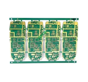
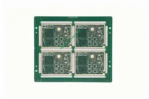
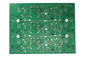
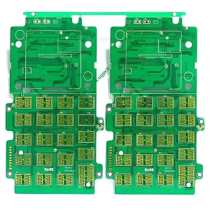
HDI-Leiterplatten werden häufig verwendet, um das Gewicht und die Gesamtgröße von Produkten zu reduzieren, sowie die elektrische Leistung von Geräten verbessern. Leiterplatten mit hoher Dichte kommen häufig vor:
- Mobiltelefone
- Touchscreen-Geräte
- Laptops
- Digitalkameras
- 4G-Netzwerkkommunikation
Zusätzlich, Dabei spielt die HDI-Leiterplattentechnologie eine entscheidende Rolle:
- Medizinische Geräte
- Verschiedene elektronische Flugzeugkomponenten
Die Möglichkeiten der Leiterplattentechnologie mit hoher Verbindungsdichte scheinen nahezu grenzenlos, bietet erhebliche Größenvorteile, Gewicht, und elektrische Leistung in einem breiten Anwendungsspektrum.