
Cet article intègre les principes fondamentaux de la conception des circuits imprimés du bus CAN dans une approche orientée ingénierie., analyse approfondie. Il commence par les tendances du marché et approfondit progressivement les points de décision techniques clés., comme la formule du coefficient de réflexion, stub length criteria, and the strategic placement of common mode chokes. It concludes with a comprehensive design checklist. Every piece of data in this article comes from authoritative sources, and every conclusion has been validated under practical operating conditions. Whether you are designing an automotive-grade ECU or laying out a long-distance industrial CAN bus, this article will help you re-examine those “millimeter-level” details that determine communication success or failure.
After reading this article, you will gain a thorough understanding of:
- Why the core of CAN bus PCB design is a millimeter-level trade-off game.
- How to ensure signal integrity in the CAN FD and CAN XL era through precise termination resistor placement, stub control, and common-mode suppression layout.
- How to eliminate hidden risks that could plague you during mass production, starting from the top-level design.
1. Introduction: CAN Communication is Everywhere, but the PCB Design Challenge Has Just Begun
From automotive cockpits to industrial production lines, CAN bus technology is experiencing unprecedented deep penetration and rapid iteration.
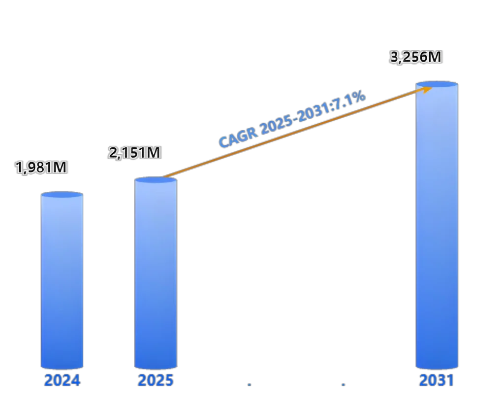
According to an industry report released by QYResearch, the global CAN bus transceiver market was valued at approximately USD 2.151 milliards dans 2024 and is projected to reach USD 3.465 milliards 2032, representing a compound annual growth rate (TCAC) of about 7.1% depuis 2026 à 2032. The overall Controller Area Network (PEUT) market was valued at approximately USD 1.981 milliards dans 2024 and is expected to reach USD 3.256 milliards 2031. Entre-temps, the CAN bus interface module market was valued at USD 1.33 milliards dans 2025 and is projected to grow at a CAGR of 7.98% to reach USD 2.28 milliards 2032. Behind these figures lies the fact that the evolution of communication technology is redefining the boundaries of physical layer design.
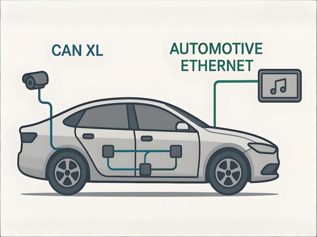
Changes in the automotive electronics sector are particularly dramatic. As of 2024, the share of traditional CAN in automotive electronic systems has dropped from over 90% dans 2018 to about 60%, while the share of CAN FD has jumped from less than 5% to about 25%. According to industry surveys, the penetration rate of CAN FD in newly launched car models in 2025 will exceed 60%. The data phase transmission rate of CAN FD can reach 8 Mbps, which is eight times that of traditional CAN (with an upper limit of 1 Mbps). CAN XL technology is also advancing rapidly, with a maximum data field length of 2024 bytes, providing a more solid physical layer foundation for low-end backbone networks and the underlying operation of high-end Ethernet protocols.
The higher the data rate, the more fatal the “details” in PCB design become. Chaque “millimeter-level” error in physical layer design can be amplified at the network level into catastrophic communication failures.
2. Termination Resistor: The Physical Logic and Pursuit of Excellence Behind 120Ω
In a CAN bus topology, the two 120Ω resistors at the physical ends of the bus are the last and most important line of defense for signal integrity.
The value of 120Ω is not arbitrary. According to the ISO 11898-2 standard, the characteristic impedance of the CAN_H and CAN_L differential pair is specified as 120Ω. This specification is perfectly consistent with the characteristic impedance of shielded or unshielded twisted pair cables widely used in the automotive industry.
In transmission line theory, the effectiveness of termination resistor matching can be measured by the reflection coefficient. The mathematical definition of the reflection coefficient (Γ) est le suivant:
Γ = (Z_L – Z_0) / (Z_L + Z_0)
OùZ_L is the load impedance (c'est-à-dire, the termination resistor), etZ_0 is the characteristic impedance (120Oh) of the transmission line (differential traces). When no termination resistor is connected at the bus end, Z_L approaches infinity, and Γ ≈ 1, meaning almost all signal energy is reflected back. When a 120Ω termination resistor is correctly connected, Z_L ≈ Z_0, then Γ ≈ 0, reflections disappear, and the waveform becomes clean.
In component selection and layout, this is a persistent battle against parasitic parameters. Chip resistors in 0603 ou 0402 packages are preferred because they have lower parasitic inductance compared to the 0805 emballer. The termination resistor and its connecting vias should be placed as close as possible to the connector or CAN transceiver pins. The path from the resistor pad to the via on the GND plane should be “short and thick” to minimize the inductance of the return path.
3. Stubs and Topology: Le “Tueur invisible” at the Millimeter Level in CAN Bus PCB Design
As CAN FD moves toward 8 Mbps and even higher data rates, le “bout” is evolving from a routine clause in design specifications into a key factor affecting system success or failure.
In a “daisy chain” topology, once the round-trip delay of each short trace segment branching off from the main bus to the transceiver exceeds 1/4 of the signal rise time, reflections begin to significantly impact signal quality. The theoretical formula for calculating stub length is as follows:
L_stub = 0.1 × t_r × v × c
Oùv is the signal propagation speed in the PCB dielectric material (environ 0.5 times the speed of lightc for FR4 material), c is the speed of light (3×10⁸ m/s), ett_r is the signal rise time.
When the rise timet_r of CAN FD shortens to 10 ns, the theoretical maximum allowable stub lengthL_stub is approximately:
L_stub = 0.1 × (10×10⁻⁹ s) × 0.5 × (3×10⁸ m/s) = 0.15 m
C'est 150 mm. For traditional CAN with a rise time of 50 ns, this value is as high as 750 mm.
Cependant, in actual working conditions — temperature drift, component aging, and the cumulative effect of reflections from multiple nodes — can severely compress this margin. Donc, the industry generally recommends controlling the stub length on the CAN bus PCB to within 100 mm (0.1 m).
Dans une conception pratique, le “daisy chain” topology must be strictly adhered to, with termination resistors placed at the physical ends of the bus. Any attempt at a “star” topology will turn every branch into an uncontrollable stub, leading to a sharp deterioration in signal quality.
4. Common Mode Choke and Split Termination: Attack and Defense in EMC
The placement of the common mode choke is the most delicate detail in the entire EMC design, testing the designer’s skill.
The correct placement order is: Connector → TVS Diode → Common Mode Choke → Termination Resistor → CAN Transceiver. The common mode choke must be placed between the termination resistor and the connector, never between the termination resistor and the transceiver. The presence of the termination resistor (120Oh) is to absorb differential mode energy on the bus. If the choke is placed after the termination resistor, its own parasitic capacitance (typically a few pF to over ten pF) will interact with the 120Ω resistor, forming unnecessary resonance at high frequencies and worsening signal quality.
In terms of component selection, a 51μH-100μH common mode choke is recommended for in-vehicle CAN applications, using an 0603 ou 0805 emballer. Murata’s DLW43SH series (with a typical DCR of 4-6Ω) is a classic and reliable choice. For higher-speed CAN FD applications, special attention needs to be paid to the choke’s self-resonant frequency (SRF), and models with an SRF higher than 100 MHz should be selected.
Split Termination is a more refined means of optimizing common-mode filtering. It uses two 60Ω resistors in series to replace a single 120Ω termination resistor, and the midpoint of the two resistors is connected to GND through a capacitor (typical value: 4.7nF to 47nF).
This RC network forms a low-pass filter, and its cutoff frequency can be estimated as:
f_c ≈ 1 / (2π × R_eq × C), oùR_eq = (R/2) = 30Ω
When C is 10nF, the cutoff frequencyf_c is approximately 530 kHz. This means that high-frequency common-mode noise on the bus can be effectively bypassed to ground through this capacitor, while the differential signal path is almost unaffected.
5. Conclusion and Design Checklist: The Final Step from Theory to Mass Production
| Check Item | Design Requirement |
|---|---|
| Impédance différentielle | 120Ω ±10% (±7% recommended for CAN FD) |
| Termination Resistor | One 120Ω at each physical bus end, 1% tolérance, 0603 ou 0402 emballer |
| Intra-Pair Skew | ≤2.54 mm (≤1 mm for CAN FD) |
| Stub Length | ≤100 mm, the shorter the better |
| Topology | Strict daisy chain, termination at both ends, star topology prohibited |
| Common Mode Choke | Located between termination resistor and connector, 51-100μH, SRF > 100 MHz |
| Reference Plane | Complete, continuous GND plane, no trace routing across split planes |
| Spacing to Other Signals | >3W or >50 mil, avoid long-distance parallel routing |
| Protection ESD | TVS near connector, junction capacitance <10 pF, strictly control total node capacitance |
| Split Termination | Optional (2×60Ω in series + 4.7nF-47nF cap to GND), enhances common-mode filtering |
| Number of Vias | ≤3 vias on CAN differential pair to avoid introducing parasitic inductance and impedance discontinuity |
| Trace Corner | Use 45° bevel or arc routing, 90° corners strictly prohibited |
All the essence of CAN bus PCB design is condensed into the rigorous execution of every detail listed above. As a professional CAN bus PCBA supplier, we have helped thousands of engineers achieve success from schematic to mass production.
To transform your CAN bus project from design drawings into reliable, mass-producible products, please contact us for professional PCBA design support and manufacturing services.
Data Citation Notes
- All cited data comes from publicly available, authoritative research reports (Research and Markets, GII Research, QYResearch, TI E2E Forum, NXP App Note, CiA publications, etc.).
- All electrical parameters and formulas have been cross-validated with mainstream sources.
- Standard citations include the standard number and year.
