
Imagine a circuit imprimé à grande vitesse as a busy data city. The vias that carry signals between layers are like underground tunnels.
According to the industry-standard approximation from IPC-2251, a typical through-hole via has a parasitic capacitance between 0.3 pF and 0.8 pF. When signal frequencies exceed 10 Gbit/s, this small number can cause reflections and delays. It can turn a perfectly designed data link into a bit error storm.
This article analyzes the causes and optimization paths of via parasitic capacitance from three physical dimensions: circuit, field, and material.
1. The Capacitance Attenuation Layer – Controlling Geometric Dimensions to Reduce Electric Field Leakage
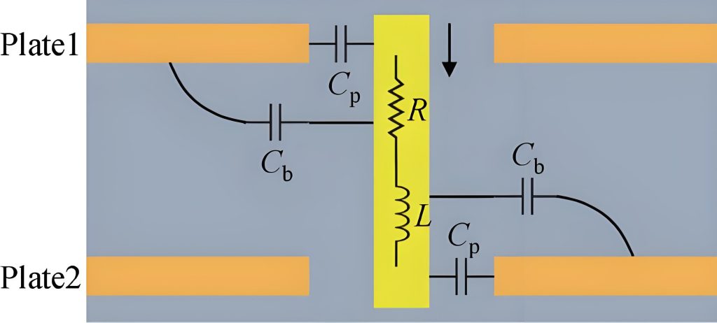
The physical origin of via parasitic capacitance lies in the coupling between the via pad and the reference ground layer.
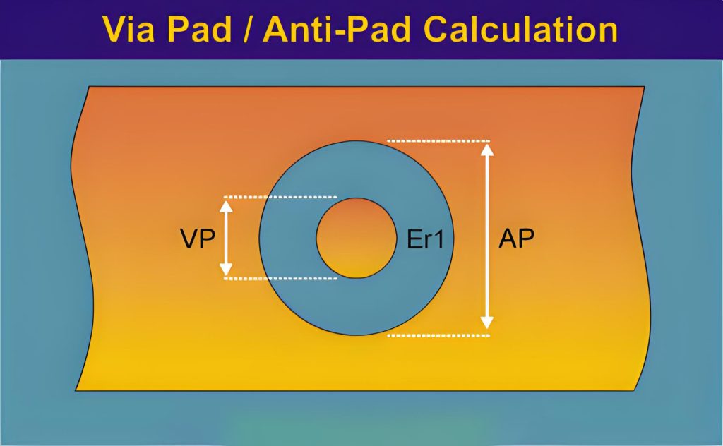
From an electromagnetic field perspective, the pad and ground plane form a parallel-plate capacitor. To reduce via parasitic capacitance, the most direct path is to shrink the effective plate area.
Industry practice follows minimum annular ring requirements. For IPC-6012 Class 3 haute fiabilité, the outer layer minimum is 2 mil, while the inner layer can be reduced to 1 mil. This minimization strategy reduces the pad diameter and effectively compresses the coupling area with the ground plane.
Increasing the hole-to-pad diameter difference provides another path to reduce capacitance. You must follow the formula:
Pad Diameter = Drill Diameter + 2 × Annular Ring
Drilling typically accounts for 30%–40% of Fabrication de circuits imprimés coût. Donc, via dimension adjustments require close coordination with economic constraints.
For antipad treatment, removing copper around the pad on specific layers increases the spatial distance between conductors. Cependant, excessive clearance may cause crosstalk on adjacent traces and discontinuity in the reference plane.
2. The Dielectric Parameter Layer – The “Signal Slowdown Zone” in Material Selection
Standard Matériau FR-4 has a relative dielectric constant Dk ≈ 4.2–4.8 at 1 GHz. À 10 GHz, the Dk value may drop by 5%–10%.
Low Dk materials (Dk ≤ 3.5) effectively reduce via parasitic capacitance because capacitance is directly proportional to the dielectric constant. Cependant, these materials cost more and require harder processing. For ordinary low-speed circuits, you do not need to adopt this solution. IPC-4101 defines the technical boundaries for material selection. High-frequency designs must refer to the relevant Slash Sheet specifications in this standard.
3. The Electromagnetic Boundary Layer – Letting Signals Pass with Precision
Controlling via stub length is a critical method for breaking through high-speed bottlenecks.
Engineering Threshold for Back Drilling
Pour 10 Gbps or higher SerDes channels, a stub length exceeding 10 mil (à propos 0.254 mm) can cause observable insertion loss notches. Commercial back drilling processes can reliably control stub length between 4 mil and 8 mil (0.1 mm to 0.2 mm).
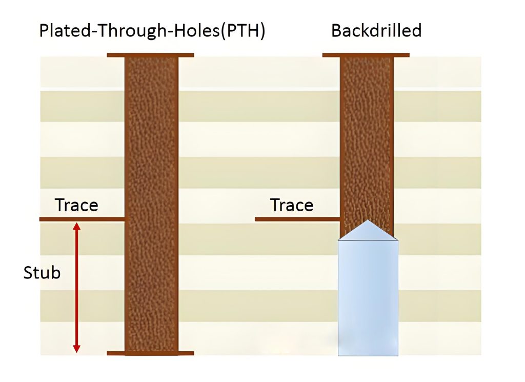
A via stub acts as an open-circuited transmission line stub. When the stub length equals one-quarter of the dielectric guided wavelength, it excites a high-Q series resonance. The return loss S11 can locally deteriorate beyond –8 dB.
Quantitative Judgment of Reflection Coefficient
The reflection coefficient formula is:
Γ = (Z₂ − Z₁) / (Z₂ + Z₁)
Où:
- Z₁ = line impedance before the reflection point
- Z₂ = line impedance after the reflection point
In an ideal case, Γ → 0 means full absorption with no reflection. Γ → ±1 means total reflection. When a via introduces additional parasitic parameters, Γ deviates from zero. Design must keep this deviation within an acceptable range through impedance control.
Via Barrel Wall Design Principles
At the microstructural level, via inner diameter, rapport d'aspect (épaisseur du panneau / diamètre du trou), and copper plating thickness directly determine via mechanical reliability. Standard hole wall copper thickness ranges from 2.5 mil to 3.0 mil. The mechanical drilling limit for hole diameter is 6 mil (0.15 mm). Laser drilling can reach 4 mil (0.1 mm). When the aspect ratio exceeds 8:1, the plating solution cannot fully penetrate the hole center, and voids or cracks rise sharply.
Cost Trade-off for Blind and Buried Vias
Blind and buried vias can reduce parasitic capacitance to 1/3 ou 1/5 of a through-hole via. Cependant, their fabrication cost per square inch is about 1.3 à 2.0 times higher than that of through-hole boards. Industry data shows that drilling accounts for 30%–40% of total PCB fabrication cost. Blind vias significantly increase this percentage due to their process complexity. Recommend using blind/buried vias only in these scenarios: system data rate ≥56 Gbps PAM4, IDH any-layer interconnect for high routing density, or small packaging areas that cannot accommodate through-holes.
Summary of Optimization Measures
The table below summarizes all solutions and their cost impact based on the source material.
| Optimization Category | Specific Measure | Cost Impact |
|---|---|---|
| Via dimension design | Reduce pad diameter; increase hole-to-pad diameter difference | Minor – but watch mechanical strength and reliability |
| Dielectric and isolation design | Increase dielectric distance; remove antipad; use low Dk material | Medium to High – low Dk material costs more |
| Via placement design | Keep away from ground plane edges; control spacing to adjacent conductors | Minor – but requires safe clearance |
| Via structure selection | Back drilling to remove stub; use blind/buried vias; reduce layer transition count | Medium to High – blind/buried vias cost 1.3–2.0x of through-holes |
Get Professional Support for Your High-Frequency Via Optimization
When your design team faces tough via optimization challenges for high-frequency signals, you need an experienced Fournisseur de PCBA. We offer precise impedance simulation quotes and high-yield back drilling samples. Our fabrication capabilities meet IPC-6012 Class 3 high reliability standards and include mature HDI via structures. Click the button to request your custom design and manufacturing support.
Références
[1] IPC-2251, Design Guide for the Packaging of High Speed Electronic Circuits, IPC, 2003.
[2] IPC-4101E/21, Specification for Base Materials for Rigid and Multilayer Printed Boards, IPC.
[3] IPC-6012D, Qualification et spécifications de performances pour les cartes imprimées rigides, IPC.
[4] IPC-D-317A4, Design Standard for Printed Board Assemblies, IPC.
[5] IPC-TM-650, Test Methods Manual, IPC.
