
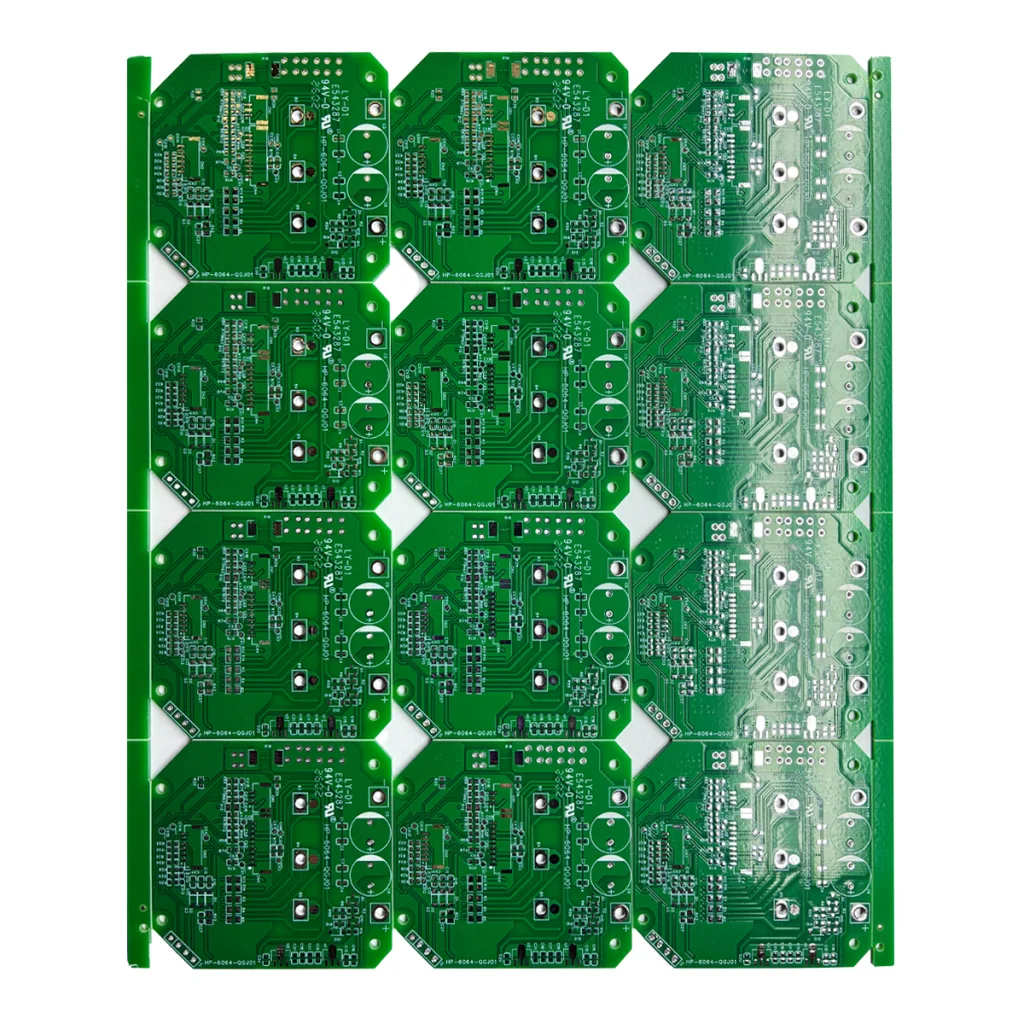
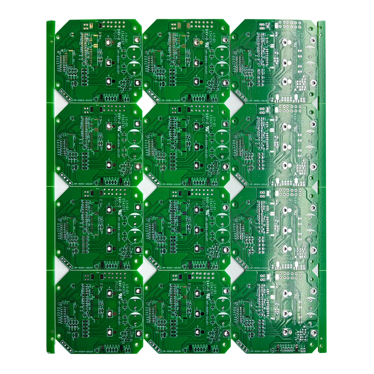
PCB double face FR-4 hautes performances Présentation du produit & Définition
Ce 2-Couche rigide Circuit imprimé (PCB) de l'UGPCB est une solution d'interconnexion électronique fondamentale et largement utilisée. Il dispose d'une norme 1.6mm épaisseur du panneau, dimensions de 224.02mm x 189 mm, et utilise des produits de haute qualité Ko FR-4 stratifié. Ce PCB double face est l'élément essentiel “colonne vertébrale” pour les conceptions électroniques, fournir des connexions électriques fiables et un support mécanique pour les composants. C'est un idéal, choix économique pour une vaste gamme de contrôles industriels, électronique grand public, et applications d'alimentation électrique.
Considérations critiques de conception
La conception réussie d'un PCB double face nécessite un équilibre entre les performances électriques et la fabricabilité. Les principales considérations comprennent:
-
Stratégie de routage: Utiliser efficacement les couches supérieure et inférieure pour le routage des traces. Trous traversants plaqués (PTH ou Vias) activer les connexions inter-couches. Une planification minutieuse de la densité des traces est cruciale pour éviter les problèmes d'intégrité du signal tels que la diaphonie.
-
Trou & Conception du tampon: Spécifiez les tailles de forets et les diamètres de tampons appropriés pour tous Vias PCB et les câbles des composants pour garantir la résistance mécanique et la fiabilité du soudage, adhérer à Normes IPC pour bague annulaire.
-
Pouvoir & Plans au sol: Alors que les avions dédiés sont absents, les concepteurs doivent élargir les traces d'alimentation et de terre ou mettre en œuvre une coulée de cuivre grillagée pour réduire l'impédance et améliorer la stabilité - un aspect clé d'une robustesse Conception de circuits imprimés.
-
Vérification des règles de conception (RDC): Avant la fabrication, vérifier rigoureusement que tous les paramètres (largeur/jeu de trace, tailles de trous) s'aligner sur les capacités du fabricant (selon les spécifications de cette carte) garantir Conception de PCB pour la fabricabilité (DFM).
Principe de fonctionnement & Structure
La fonctionnalité de ceci circuit imprimé double couche découle de sa structure en couches:
-
Construction: Le noyau est constitué d'un Couche diélectrique isolante FR-4, recouvert d'une feuille de cuivre (typiquement 1 once) des deux côtés. Le cuivre indésirable est éliminé pendant Fabrication de circuits imprimés, former les traces de circuit souhaitées.
-
Interconnexion électrique: Les circuits sur les deux couches sont connectés verticalement via Trous traversants plaqués (PTH), créé à travers forage mécanique suivi de dépôt de cuivre chimique et électrolytique.
-
Protection des surfaces: Le Nivellement de soudure à air chaud sans plomb (HASL) la finition appliquée sur les plots de cuivre exposés empêche l'oxydation et assure une excellente soudabilité pour l'assemblage des composants.
Classement du produit & Matériels
Selon les spécifications fournies, ce produit est classé avec précision comme suit:
-
Par nombre de couches: PCB double face ou 2-PCB de couche.
-
Par rigidité du substrat: PCB rigide.
-
Par matériau de base: Carte FR-4. Spécifiquement, FR-4 du “Ko” marque, un stratifié de verre époxy connu pour son isolation électrique supérieure, résistance mécanique, et le retard de la flamme (UL94-V0).
-
Par finition de surface: PCB HASL sans plomb.
-
Par complexité d’application: Standard, PCB de qualité industrielle à usage général.
Performance & Caractéristiques clés
Tirer parti des matériaux et des processus spécifiés, ce PCB offre les avantages de performance de base suivants:
-
Mécanique fiable & Performance électrique: Le Matériel KB FR-4 offre une constante diélectrique stable et un faible facteur de dissipation pour l'intégrité du signal. L'épaisseur standard de 1,6 mm offre une excellente résistance à la flexion et aux vibrations.
-
Interconnexions fiables: Le Finition de surface HASL sans plomb fournit un appartement, revêtement hautement soudable compatible avec les procédés de brasage à la vague et à la main.
-
Stabilité thermique supérieure: Le substrat FR-4 résiste aux températures de soudure standard et offre une température de fonctionnement continue élevée, convient à la plupart électronique industrielle environnements.
-
Rentabilité élevée: Par rapport aux cartes multicouches, PCB double face offre nettement inférieure Coût de fabrication des PCB et des délais de livraison plus courts, représentant une solution matérielle économique.
-
Conformité environnementale: Le HASL sans plomb le processus est conforme aux directives internationales telles que RoHS.
Processus de fabrication détaillé
L'UGPCB adhère à un strict, de haute qualité Processus de fabrication des PCB:
-
Ingénierie & CAME: Analyse de fichier Gerber, Vérification DFM, et génération de photoplots.
-
Panélisation: Couper le grand FR-4 stratifié cuivré en panneaux de production.
-
Forage: Perçage CNC des trous de composants et Vias PCB.
-
Métallisation des trous: Désenduire, dépôt chimique de cuivre, et placage de cuivre électrolytique pour former des conducteurs Trous traversants plaqués (PTH).
-
Modélisation: Application de photorésist, exposition, développement pour transférer l'image du circuit.
-
Gravure: Suppression du cuivre indésirable pour former des traces de circuit précises.
-
Masque de soudure & Écran à soigneux: Application du masque de soudure LPI (typiquement vert) et impression de légende.
-
Finition de surface: Candidature HASL sans plomb revêtement sur les tampons exposés.
-
Routage & Tests électriques: Profilage jusqu'au contour final de la carte et réalisation de tests électriques (Sonde volante ou Test de luminaire).
-
Inspection finale & Conditionnement: Complet Inspection optique automatisée (Zone d'intérêt), vérification dimensionnelle, et sous vide, emballage résistant à l'humidité.
Applications principales & Cas d'utilisation
Cette spécification de PCB FR-4 double face est largement déployée dans fiable et économique applications:
-
Systèmes de contrôle industriels: Contrôleurs API, cartes d'entraînement de moteur, modules d'interface de capteur.
-
Unités d'alimentation: Alimentations à découpage (SMPS), Systèmes UPS, Cartes de commande LED.
-
Electronique grand public: Tableaux de commande d'appareils (CA, machines à laver), contrôleurs de maison intelligente, équipement audio.
-
Électronique automobile: Modules de contrôle du corps (BCM), contrôleurs d'éclairage, systèmes d'infodivertissement non critiques.
-
Équipement de télécommunications: Modules fonctionnels dans les routeurs, commutateurs.
-
Test & Instruments de mesure: Panneaux d'acquisition de données et d'affichage pour équipements.

Pourquoi choisir l'UGPCB pour vos besoins en PCB double face?
Partenariat avec les garanties UGPCB:
-
Fabrication de précision: Respect strict d'une épaisseur de 1,6 mm, 224.02dimensions x189mm, et Matériau FR-4 caractéristiques.
-
Excellence des processus: Standardisé Production de PCB HASL sans plomb garantit la cohérence et la fiabilité d’un lot à l’autre.
-
Assistance technique experte: Notre équipe fournit un accompagnement complet, depuis Conception de circuits imprimés revoir à la consultation de production.
-
Livraison clé en main rapide: Nous offrons des délais de livraison compétitifs pour les doubles couches standards Prototypes de PCB et cycles de production.
Prêt à démarrer votre projet? Contactez l'UGPCB dès aujourd'hui pour un devis compétitif et une assistance experte.. Laissez-nous être votre confiance Fabricant de PCB et partenaire pour le succès.


