je. Présentation du produit
La carte PCB à trou traversant double face UGPCB est une carte rigide à 2 couches haute performance circuit imprimé construit sur un substrat verre-époxy FR-4 utilisant un trou traversant plaqué (PTH) technologie. Le conseil mesure 86.9 × 73.58 mm avec une épaisseur de 1.0 mm, épaisseur de feuille de cuivre de 1/1 once (35 μm sur les couches externe et interne), et un nivellement de soudure à air chaud sans plomb (HASL) finition de surface. Le masque de soudure est vert, et la légende sérigraphiée est blanche.
Un PCB traversant double face (circuit imprimé double face) comporte des circuits conducteurs des deux côtés du substrat isolant, avec des trous traversants plaqués permettant l'interconnexion électrique entre les deux couches. Comparé aux PCB simple face, les PCB double face offrent une densité de routage 60 à 80 % plus élevée et prennent en charge des conceptions de circuits plus complexes. UGPCB, soutenu par des systèmes de qualité certifiés ISO et des processus de fabrication conformes à l'IPC, fournit des PCB traversants double face de haute qualité et clé en main PCB services aux fabricants d'électronique du monde entier.
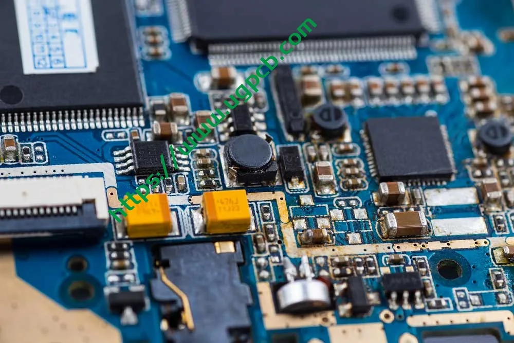
II. Définition du produit et spécifications techniques
Selon IPC-6012F Qualification et spécifications de performances pour les cartes imprimées rigides (publié en septembre 2023), le PCB traversant double face est classé comme une carte imprimée rigide avec des trous traversants plaqués (Taper 2). Sa caractéristique principale est la connexion électrique entre les conducteurs des deux côtés à travers des parois perforées cuivrées.. UGPCB fabrique ce produit en totale conformité avec IPC-6012F et répond à la classe 2 exigences de performance (équipement électronique de service dédié).
Spécifications clés:
| Paramètre | Spécification |
|---|---|
| Matériau du substrat | FR-4 (Ignifuge UL 94 V-0) |
| Nombre de couches | 2 couches (double face) |
| Épaisseur du panneau | 1.0 mm |
| Dimensions de la carte | 86.9 × 73.58 mm |
| Diamètre minimum du trou | 0.236 mm |
| Largeur de ligne minimale / Espacement | 0.32 × 0.37 mm |
| Épaisseur de la feuille de cuivre | 1/1 once (environ. 35 μm de chaque côté) |
| Finition de surface | HASL sans plomb (Nivellement de la soudure à air chaud) |
| Masque de soudure / Légende | Masque de soudure vert / Sérigraphie blanche |
III. Directives de conception
3.1 Sélection des matériaux de substrat — Valeur technique du FR-4
FR-4 est une désignation de qualité ignifuge établie par la National Electrical Manufacturers Association (NON). Les lettres “FR” signifie ignifuge, et le numéro “4” désigne un système de résine époxy renforcé de tissu de verre tissé. Pour IPC-4101 Spécification des matériaux de base pour les cartes imprimées rigides et multicouches, FR-4 Grade A1 représente le niveau de performance de base avec une résistance mécanique optimale, propriétés électriques, et fiabilité à long terme.
Indicateurs de performance clés du FR-4 (Source: IPC-4101 et normes industrielles):
-
Température de transition du verre (Tg): 130–140°C (norme FR-4)
-
Constante diélectrique (Ne sait pas) @ 1 GHz: 4.2–4,5
-
Facteur de dissipation (Df) @ 1 GHz: ≤ 0.020
-
Cote d'inflammabilité: UL 94 V-0
-
Absorption d'eau (24 heures): ≤ 0.10%
Le FR-4 reste le matériau de substrat prédominant dans l'industrie des PCB car il offre un équilibre exceptionnel de résistance mécanique., isolation électrique, stabilité dimensionnelle, et la transformabilité.
3.2 Normes de conception de circuits selon IPC-2221
Pour IPC-2221 Norme générique sur la conception des cartes imprimées, la conception de la largeur du conducteur doit tenir compte de la capacité de transport de courant, augmentation de la température, et épaisseur de cuivre. La formule de capacité de transport de courant IPC-2221 est:
Je = k · ΔT^0,44 · A^0,725
Où:
-
I = Capacité de transport de courant maximale (UN)
-
k = Constante empirique (0.048 pour couches externes, 0.024 pour les couches internes)
-
ΔT = Élévation de température admissible (° C)
-
A = Section transversale du conducteur (mil²), où A = W × T
Le produit de l'UGPCB présente une largeur de ligne de 0.32 mm (environ. 12.6 mil), espacement des lignes de 0.37 mm (environ. 14.6 mil), et une épaisseur de cuivre de 1 once (35 µm). Pour un tracé en couche externe avec une élévation de température de 10°C:
UNE = 0.32 mm × 0.035 mm = 0.0112 mm² ≈ 17.36 mil²
Je = 0.048 × 10 ^ 0,44 × 17,36 ^ 0,725 ≈ 0.048 × 2.75 × 7.82 ≈ 1.03 UN
Cette largeur de conducteur supporte environ 1 Un courant, répondant aux besoins de transmission de puissance et de signal de la plupart des équipements électroniques grand public et de contrôle industriel. IPC-2221 recommande de limiter l'augmentation maximale de la température à 10°C ou 20°C pour préserver la durée de vie des PCB.
3.3 Conception du diamètre du trou et du rapport d’aspect
Le rapport hauteur/largeur d'un trou traversant est une mesure critique pour évaluer la difficulté de forage et de métallisation du trou.. La formule est:
Rapport d'aspect = épaisseur de la planche / Diamètre du trou percé
Pour le produit UGPCB avec 1.0 mm d'épaisseur de panneau et 0.236 mm diamètre minimum du trou:
Rapport hauteur/largeur = 1.0 / 0.236 ≈ 4.24:1
Ce rapport hauteur/largeur est bien inférieur à la limite supérieure recommandée par l'industrie. 10:1 et le seuil de conception conservateur de 8:1. Cela indique une faible difficulté de perçage et de métallisation, taux de rendement élevés, des coûts maîtrisés, et une fiabilité traversante assurée.
3.4 Référence de conception de modèle de terrain
Pour IPC-7351 Exigences génériques pour la conception de montage en surface et la norme de configuration du terrain, la conception du modèle de pastille doit garantir une formation adéquate du filet de soudure et répondre à la soudabilité, inspectabilité, et exigences de retouche. Pour composants traversants, le diamètre du plat est généralement recommandé entre 1,8 et 2,2 fois le diamètre du trou pour garantir une largeur d'anneau annulaire suffisante.
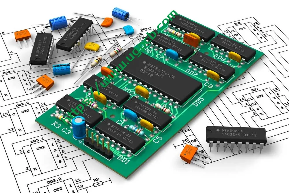
IV. Principe de fonctionnement
Le PCB traversant double face fonctionne sur trois technologies de base:
1. Routage double face — Des motifs de circuits conducteurs sont gravés sur les surfaces supérieure et inférieure du substrat isolant FR-4., permettant le placement des composants des deux côtés. Cela augmente considérablement la densité des circuits et la flexibilité de conception.
2. Trou traversant plaqué (PTH) Interconnexion — Après perçage, le dépôt autocatalytique de cuivre et le placage électrolytique de cuivre créent une couche conductrice sur les parois du trou. Cela crée une faible résistance, connexions électriques très fiables entre les couches supérieure et inférieure. Par classe IPC-6012F 2, l'épaisseur moyenne minimale du cuivre plaqué sur les parois des trous doit être ≥ 20 µm.
3. Assemblage de composants et soudure — Les composants sont montés à travers le trou (Tht) ou montage en surface (CMS) techniques et connecté électriquement par refusion ou brasage à la vague, produire un PCBA entièrement fonctionnel (Assemblage de la carte de circuit imprimé) module.
V. Classement du produit
Selon le système de classification IPC-6012F pour les cartes imprimées rigides, Le produit de l’UGPCB est classé comme suit:
| Dimension de classification | Catégorie |
|---|---|
| Par construction | Carte imprimée rigide avec trous traversants plaqués, Double face (Type IPC-6012F 2) |
| Par classe de performances | Classe 2 (Équipement électronique de service dédié) |
| Par matériau de substrat | Stratifié de tissu de verre époxy FR-4 (IPC-4101/21) |
| Par nombre de couches | 2-Conseil de calque |
| Par finition de surface | HASL sans plomb |
| Par indice d'inflammabilité | UL 94 V-0 |
Par domaine d'application, ce produit entre dans la catégorie PCB double face de qualité industrielle générale catégorie, adapté à l'électronique grand public, contrôles industriels, équipement de communication, adaptateurs de puissance, et autres applications de fiabilité moyenne.
Vi. Composition des matériaux
6.1 Substrat — Stratifié cuivré FR-4
FR-4 est un stratifié époxy renforcé de verre composé de tissu de verre tissé de qualité électronique comme renfort et de résine époxy comme liant., consolidé sous haute température et pression. C'est UL 94 V-0 L'indice d'inflammabilité signifie que lors de l'essai de combustion verticale, le matériau s'éteint automatiquement à l'intérieur 10 secondes après chacune de deux applications de flamme de 10 secondes, sans gouttes enflammées qui enflamment le coton.
6.2 Feuille de cuivre — 1/1 once
Une once (1 once) de feuille de cuivre a une épaisseur de 35 µm (1.37 mil). UGPCB utilise 1 Cuivre OZ sur les deux couches externes (désigné 1/1 once), assurant une capacité de transport de courant et une conductivité égales des deux côtés.
6.3 Finition de surface — HASL sans plomb
Le HASL sans plomb consiste à immerger le PCB dans de la soudure sans plomb fondue (généralement Sn-Cu, Sn-Cu-Ni, ou alliages Sn-Ag-Cu), puis à l'aide de couteaux à air chaud haute pression pour niveler et éliminer l'excès de soudure. Cela produit un uniforme, revêtement protecteur soudable sur les surfaces en cuivre. Le processus est conforme aux exigences IPC-6012F et aux directives environnementales RoHS.
6.4 Masque de soudure et légende
-
Masque de soudure vert — Couvre toutes les zones de circuit à l'exception des pads, assurer l'isolation, protection contre l'oxydation, et prévention des courts-circuits.
-
Légende de la sérigraphie blanche — Identifie les indicateurs de référence des composants, marqueurs de polarité, numéros de pièces de la carte, et niveaux de révision pour faciliter l'assemblage et le débogage.
VII. Performances du produit
7.1 Performance électrique
| Paramètre de performances | Valeur | Norme de référence |
|---|---|---|
| Constante diélectrique (Ne sait pas) @ 1 GHz | 4.2–4,5 | CIB-4101 |
| Facteur de dissipation (Df) @ 1 GHz | ≤ 0.020 | CIB-4101 |
| Résistance d'isolation | ≥ 10 ^ 12 Ω | IPC-6012F |
| Tension de tenue diélectrique | Par rigidité diélectrique | IPC-6012F |
7.2 Performances mécaniques
| Paramètre de performances | Valeur | Norme de référence |
|---|---|---|
| Épaisseur du panneau | 1.0 mm ± 10% | IPC-6012F |
| Résistance au pelage du cuivre | ≥ 1.1 N/mm | IPC-6012F |
| Cote d'inflammabilité | UL 94 V-0 | Norme UL |
| Tg (Température de transition du verre) | 130–140°C | CIB-4101 |
7.3 Fiabilité
Par classe IPC-6012F 2 exigences, le produit doit passer les vérifications de fiabilité suivantes:
-
Test de contrainte thermique (288° C, 10 secondes, pas de délaminage ni de cloquage)
-
Test d'adhérence du cuivre traversant plaqué (épaisseur moyenne minimale du cuivre dans la paroi du trou ≥ 20 µm)
-
Test de soudabilité
-
Test de continuité électrique et de résistance d'isolement
VIII. Structure du produit
Le PCB traversant double face de l'UGPCB présente une construction symétrique à 2 couches. De haut en bas:
-
Couche de légende supérieure (Sérigraphie blanche)
-
Couche supérieure de masque de soudure (Encre verte)
-
Couche supérieure de feuille de cuivre (1 once, 35 µm)
-
Substrat isolant FR-4 (1.0 mm épaisseur)
-
Couche inférieure de feuille de cuivre (1 once, 35 µm)
-
Couche de masque de soudure inférieure (Encre verte)
-
Couche de légende inférieure (Sérigraphie blanche)
-
Trous traversants plaqués (PTH) — Couvre toute l'épaisseur du panneau avec des parois de trous plaquées cuivre permettant l'interconnexion entre les couches
IX. Caractéristiques du produit
-
Haute densité de routage — Le routage double face offre une densité 60 à 80 % plus élevée que celle des cartes simple face, prenant en charge des conceptions de circuits plus complexes.
-
Interconnexion traversante hautement fiable — Trou traversant plaqué (PTH) la technologie garantit une fiabilité électrique à long terme entre les couches, avec une épaisseur de cuivre dans la paroi du trou répondant à la classe IPC-6012F 2 exigences (≥ 20 µm en moyenne).
-
Excellente ignifuge — Le substrat FR-4 est conforme à UL 94 V-0 cote d'inflammabilité, assurer la sécurité dans des conditions de fonctionnement anormales.
-
Sans plomb et respectueux de l'environnement — La finition de surface HASL sans plomb est conforme aux directives environnementales RoHS.
-
Capacité de circuit à pas fin — Largeur de trait minimale de 0.32 mm et espacement minimum de 0.37 mm accueillir moyen- aux conceptions de circuits haute densité.
-
Stabilité dimensionnelle supérieure — Faible absorption d'eau du FR-4 (≤ 0.10%) garantit un changement dimensionnel minimal dans les environnements humides, préserver la précision de l'assemblage.
-
Processus de fabrication mature - Avec 1.0 mm d'épaisseur de panneau et 0.236 mm diamètre minimum du trou, le rapport hauteur/largeur de seulement 4.24:1 permet des processus matures, rendements élevés, et des délais courts.
X. Flux de processus de fabrication
Processus de fabrication de circuits imprimés traversants double face standard de l'UGPCB:
1. Inspection des matériaux entrants → Vérifier l'épaisseur du stratifié cuivré FR-4, qualité de la feuille de cuivre, et défauts visuels.
2. Coupe → Couper le stratifié cuivré grand format à la taille du panneau de travail (86.9 × 73.58 mm).
3. Forage → Utilisez des perceuses CNC de haute précision pour percer tous les trous traversants selon le fichier de perçage Gerber (diamètre minimal 0.236 mm).
4. Trou traversant plaqué (PTH) → Déposer une fine couche de germes de cuivre sur les parois du trou par dépôt autocatalytique de cuivre.
5. Placage de panneaux → Plaquer électrolytiquement du cuivre pour former du cuivre dans les parois des trous et en surface jusqu'à l'épaisseur cible (1 once).
6. Transfert de motif → Film sec stratifié, exposer, et se développer pour former le motif de circuit résistant.
7. Gravure → Gravez le cuivre non protégé pour former le modèle de circuit final.
8. Décapage → Retirez le film sec résistant des traces du circuit.
9. Application du masque de soudure → Appliquer l'encre de masque de soudure verte, exposer, et développer pour exposer les coussinets.
10. Finition de surface → HASL sans plomb.
11. Impression de légende → Légende sérigraphiée en blanc.
12. Routage / Coupe en V → Routage CNC jusqu'au contour final de la carte.
13. Tests électriques → Test de sonde volante ou de luminaire pour vérifier l'intégrité de l'ouverture/du court-circuit.
14. Contrôle de la qualité final (FQC) → Inspection visuelle, échantillonnage dimensionnel, et emballage pour l'expédition.
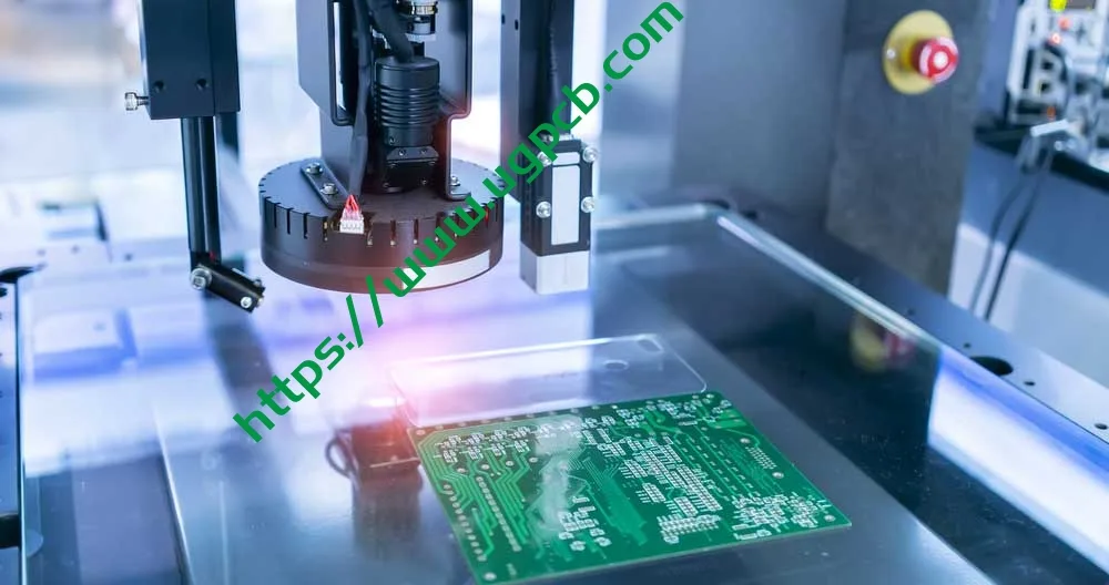
XI. Scénarios d'application
Cartes PCB FR-4 à trou traversant double face UGPCB, avec leurs performances équilibrées et leurs processus matures, sont largement utilisés dans:
11.1 Electronique grand public
-
Adaptateurs secteur et chargeurs
-
Tableaux de commande d'appareils électroménagers
-
Appareils domestiques intelligents
11.2 Commandes industrielles
-
Contrôleurs logiques programmables PLC
-
Modules de puissance industriels
-
Instrumentation et compteurs
11.3 Équipement de communication
-
Routeurs et commutateurs
-
Modules de communication
-
Appareils de conversion de signaux
11.4 Électronique automobile
-
Chargeurs embarqués
-
Modules de contrôle du corps (non critique pour la sécurité)
-
Systèmes d'infodivertissement
11.5 Dispositifs médicaux
-
Cartes auxiliaires pour moniteur patient
-
Équipement médical portable (Classe 2 en vigueur)
XII. Avantages du produit et guide de sélection
12.1 Pourquoi choisir les PCB traversants double face UGPCB?
-
Contrôle de processus conforme à l'IPC — De la sélection des matériaux aux produits finis, conformité totale avec IPC-6012F, CIB-4101, et d'autres normes internationales.
-
Fabrication de haute précision — Diamètre minimum du trou de 0.236 mm et une largeur de trait minimale de 0.32 mm rencontrer moyen- aux exigences de conception haute densité.
-
Conformité environnementale — La finition de surface HASL sans plomb est conforme à RoHS 2.0 directive.
-
Fiabilité éprouvée — Le substrat FR-4 est validé sur le marché depuis des décennies avec des performances constantes.
-
Livraison rapide — Les spécifications standard contiennent de nombreuses matières premières, garantir des délais de livraison fiables.
12.2 Référence de sélection
Les PCB traversants double face UGPCB sont le choix idéal lorsque votre projet répond à ces critères:
-
Complexité de circuit modérée qui 2 les couches peuvent accueillir
-
Fréquence de fonctionnement ci-dessous 1 GHz (FR-4 fonctionne parfaitement dans cette gamme)
-
Environnement de fonctionnement à long terme ne dépassant pas 120°C
-
Applications sensibles aux coûts exigeant une valeur élevée
XIII. Demander un devis
L'UGPCB s'engage à fournir des services de fabrication de PCB de haute qualité et des services PCBA clés en main à ses clients du monde entier.. Que vous ayez besoin de circuits imprimés traversants double face de spécifications standard ou d'exigences personnalisées (épaisseur de panneau spéciale, poids de cuivre, finition de surface, contrôle d'impédance, etc.), L’équipe d’experts de l’UGPCB fournit un soutien complet depuis la conception technique jusqu’à la production en série.
Obtenez un devis aujourd'hui:
-
Soumettre des fichiers Gerber + spécifications — recevez un devis dans les 24 heures
-
Accompagnement du prototype à la production en grande série
-
Conception gratuite pour la fabrication (DFM) revoir
Contacter l'UGPCB:
📧 Demandes de vente: [sales@ugpcb.com]
🌐 Site Internet: [www.ugpcb.com]
XIV. Déclaration de source de données
Les normes et données citées dans ce document proviennent des organisations faisant autorité suivantes:
-
IPC (Association reliant les industries électroniques): IPC-6012F Qualification et spécifications de performances pour les cartes imprimées rigides (Septembre 2023); CIB-4101 Spécification des matériaux de base pour les cartes imprimées rigides et multicouches; CIB-2221 Norme générique sur la conception des cartes imprimées; CIB-7351 Exigences génériques pour la conception de montage en surface et la norme de configuration du terrain
-
UL (Laboratoires souterrains): UL 94 Norme pour les tests d'inflammabilité des matériaux plastiques pour les pièces d'appareils et d'appareils
-
NON (Association nationale des fabricants d'électricité): Définition de la qualité du matériau FR-4
-
Données techniques conformes aux normes de l'industrie: Constante diélectrique FR-4, facteur de dissipation, et d'autres paramètres de propriétés matérielles