
PCB rigide standard UGPCB à 2 couches: Cartes de circuits imprimés FR-4 fiables de 1,6 mm pour les applications exigeantes
Au cœur de l'électronique moderne, le Circuit imprimé (PCB) agit comme plate-forme fondamentale, interconnecter les composants et acheminer les signaux avec précision. UGPCB PCB rigide standard à 2 couches, construit avec un robuste 1.60mm épaisseur et performant Matériau FR-4 TG150, représente l'équilibre optimal de durabilité, performance électrique, et rentabilité pour une large gamme d'applications. Ce PCB double face est une solution éprouvée pour les prototypes et les appareils électroniques de complexité moyenne.
Définition du produit & Classification
Classement Technique:
-
Par nombre de couches: PCB double face / PCB à deux couches
-
Par rigidité du substrat: PCB rigide
-
Par matériau de base: Verre époxy (FR-4) PCB
-
Par indice d'inflammabilité: UL94V-0 (inhérent au FR-4)
-
Par compatibilité d'assemblage: Technologie à travers (Tht) et technologie de montage en surface (CMS) PCB compatible.
Ce produit est un circuit imprimé double face construit avec un stratifié cuivré des deux côtés d'un noyau isolant FR-4. La connexion électrique entre les couches est réalisée via des trous traversants plaqués (PTH). Le 1.60mm (environ 1/16 pouce) épaisseur du panneau est une norme de l'industrie, offrant une excellente stabilité mécanique.
Construction & Spécifications de matériau
Empilement des couches:
Ce 2 PCB rigide en couche la structure est la suivante (de haut en bas):
-
Masque de soudure supérieur (Blanc): Couche isolante pour éviter les ponts de soudure.
-
Couche de cuivre supérieure (1 once, ~35µm): Gravé pour former des traces et des tampons conducteurs.
-
Substrat isolant (FR-4, Tg150): Fournit un support mécanique et une isolation électrique.
-
Couche de cuivre inférieure (1 once, ~35µm): Gravé pour former un circuit de couche inférieure.
-
Masque de soudure inférieur (Blanc): Couche protectrice isolante.
-
Légende de la sérigraphie (Noir): Désignateurs de composants, logos, et marquages.
Matériaux clés:
-
Stratifié de base: FR-4TG150. Cela désigne un stratifié époxy renforcé de verre ignifuge avec une température de transition vitreuse (Tg) de 150°C. Il offre une résistance mécanique supérieure, isolation électrique, et fiabilité thermique pour un circuit imprimé rigide, ce qui en fait le choix le plus rentable de l’industrie.
-
Feuille de cuivre: Standard 1 once (once) Cuivre électrodéposé pour une conductivité et une capacité de transport de courant optimales.
-
Finition de surface: Nivellement de soudure à air chaud sans plomb (HASL). Un produit rentable et fiable Finition de surface du PCB qui offre une excellente soudabilité, bonne durée de conservation, et une protection robuste contre l'oxydation.
-
Encres: Encre de masque de soudure blanche photo-imageable de haute qualité et encre de sérigraphie époxy noire durable.
(Suggestions d'images: Schéma en coupe de l'empilement de PCB)
Tout prendre: Diagramme en coupe détaillé d'un 2 couche de PCB rigide montrant du cuivre, Noyau FR-4, et couches de masque de soudure.
Directives de conception & Principe opérationnel
Considérations critiques de conception:
-
Via la conception: Maximisez l'espace de routage de votre double face Conception de circuits imprimés en plaçant stratégiquement des trous traversants plaqués (PTH) pour les connexions inter-couches.
-
Largeur de trace / espacement: Pour 1oz de cuivre, une trace/espace minimum standard est de 6 mil/6 mil (~0,15 mm) pour garantir une fabricabilité fiable et une capacité actuelle.
-
Tampon & Anneau annulaire à trou: Assurer une taille de tampon adéquate par rapport au trou de forage pour garantir une connexion solide pour Assemblage de circuits imprimés et fiabilité.
-
Masque de soudure & Écran à soigneux: Le masque de soudure blanc facilite l'inspection visuelle pendant Assemblage SMT, tandis que la sérigraphie noire claire est cruciale pour Prototypage PCB et réparation.
Principe opérationnel:
Un PCB ne génère pas de fonction mais la permet grâce à ses voies conductrices prédéfinies. Les traces de cuivre gravées remplacent le câblage discret, assurer les connexions électriques entre les composants. Le substrat isolant FR-4 évite les courts-circuits. Plaqué à travers les trous (PTH) servir de conduits verticaux, reliant le haut et le bas Couches de cuivre PCB, doublant ainsi la zone de routage disponible par rapport à une carte simple face et augmentant la flexibilité de conception.
Caractéristiques de performance & Avantages
-
Haute fiabilité: Le Substrat FR-4 TG150 assure des performances stables dans des environnements inférieurs à sa Tg, offrant une excellente stabilité thermique et mécanique pour un circuit imprimé rigide.
-
Excellentes propriétés électriques: La faible constante diélectrique et le faible facteur de dissipation répondent aux exigences d'intégrité du signal de la plupart des circuits numériques et analogiques..
-
Haute fabricabilité: Le 1.6mm PCB standard épaisseur et HASL sans plomb les processus sont matures, assurer un rendement élevé, contrôle des coûts, et des délais rapides.
-
Soudabilité supérieure: La finition HASL offre un aspect plat, surface mouillable idéale pour les deux soudure traversante et Processus de brasage SMT.
-
Identification claire: Le masque de soudure blanc à contraste élevé avec légende noire facilite l'efficacité PCB inspection, essai, et retravailler.
-
Conformité environnementale: La finition HASL sans plomb est conforme à RoHS et à d'autres directives environnementales.
Flux de processus de fabrication standard
L'UGPCB adhère aux normes IPC dans l'ensemble de ses activités. Processus de fabrication des PCB:
Panelisation → Forage → Dépôt autocatalytique de cuivre → Stratification de film sec & Imagerie → Placage de cuivre → Gravure → Application de masque de soudure & Durcissement → Sérigraphie → Finition de surface (HASL sans plomb) → Profilage/Routage → Tests électriques (Sonde volante) → Inspection optique automatisée finale (Zone d'intérêt) → Emballage & Expédition.
Applications principales & Cas d'utilisation
Ce polyvalent PCB rigide à deux couches est largement utilisé dans les industries qui exigent un équilibre entre fiabilité et valeur:
-
Commandes industrielles: Interfaces automates, modules de capteurs, entraînements à moteur, Cartes contrôleur IHM.
-
Electronique grand public: Contrôleurs d'appareils intelligents, amplificateurs audio, alimentations, kits pédagogiques.
-
Télécommunications: Cartes périphériques routeur/switch, Modules d'antenne RF, unités de surveillance de réseau.
-
Électronique automobile: Systèmes d'infodivertissement, modules de commande d'éclairage, modules de contrôle du corps (non critique pour la sécurité).
-
Électronique de puissance: PCB pour compteurs intelligents, Cartes de contrôle UPS, circuits d'onduleur solaire.
-
Test & Mesures: Cartes d'acquisition de données, panneaux de commande des instruments, cartes de testeur portables.
Pourquoi choisir l'UGPCB pour vos besoins en PCB à 2 couches?
Choisir l'UGPCB, c'est s'associer à un partenaire fiable Fabricant de PCB engagé envers la qualité. Nous sommes spécialisés dans Prototype de PCB et production en moyenne série, mise en œuvre de tests électriques rigoureux et d'une inspection basée sur IPC-A-600 sur chaque carte. Du simple 2 panneaux de couches aux conceptions multicouches complexes, Nous fournissons un expert Conception de PCB pour la fabrication (DFM) un soutien et une chaîne d’approvisionnement rationalisée.
Contactez-nous dès aujourd'hui pour un devis compétitif et un délai de livraison rapide pour votre projet de PCB FR-4 2 couches 1,6 mm!
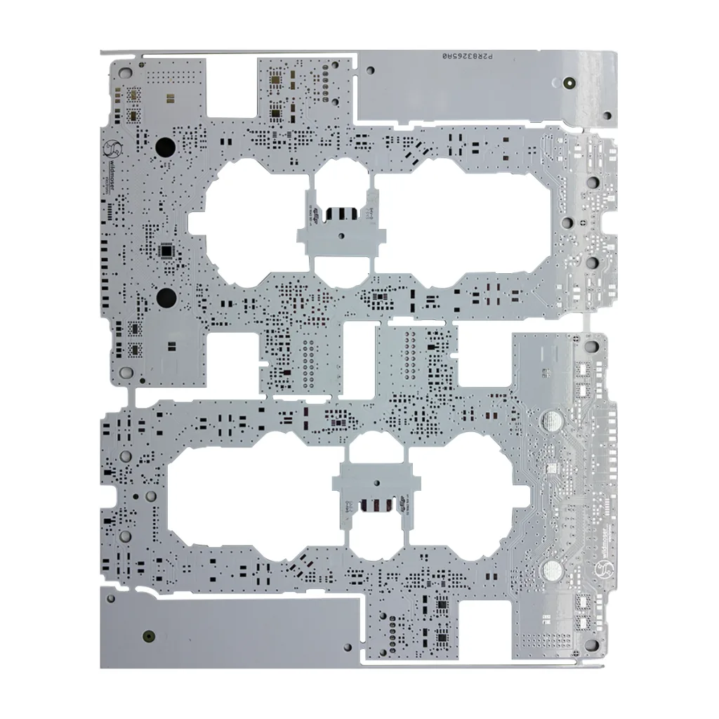
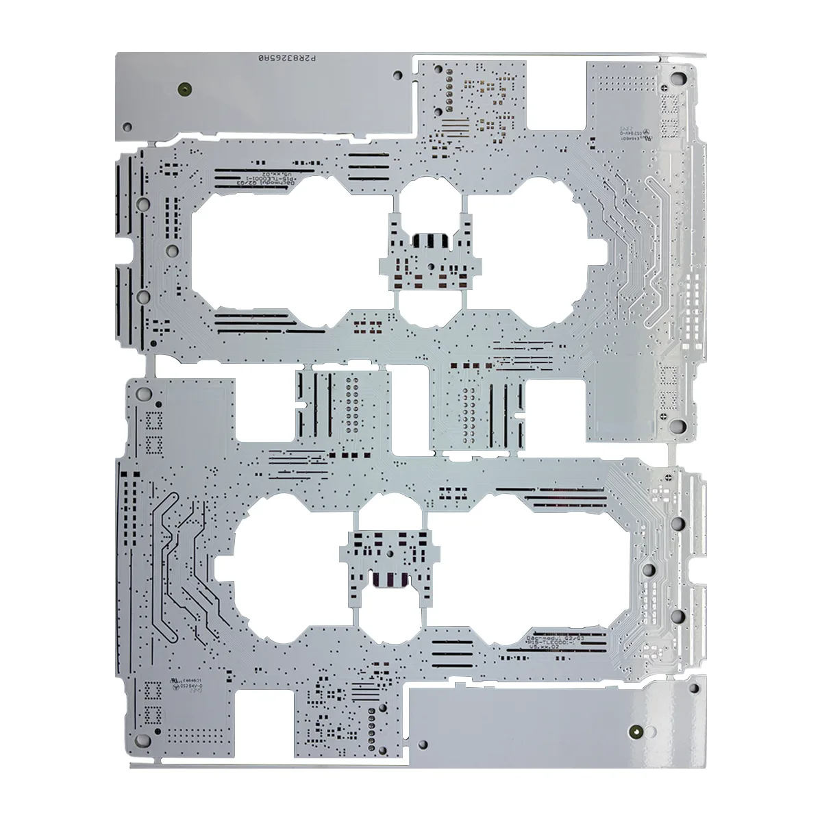
(Suggestions d'images: Galerie de PCB finis avec différents designs)
Tout prendre: Galerie de divers 2 Exemples de PCB rigides en couche fabriqués par UGPCB avec masque de soudure blanc.


