

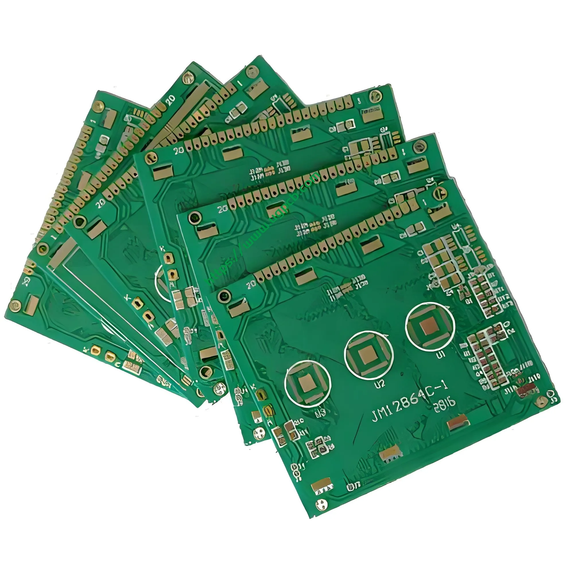
Présentation du produit: A High-Reliability PCB Solution for LCD Display Driving
L'UGPCB présente leLCD Liquid Crystal Display PCB Circuit Board (Modèle: UGPCB-LCD-001), une haute performance2-layer rigid FR-4 printed circuit board engineered specifically for liquid crystal display driving applications. This product uses Kingboard KB6165F high-end copper-clad laminate as the base material, with a board thickness of 1.6 mm et 1 feuille de cuivre d'une once (environ 35 µm). The surface finish employs theACCEPTER (Nickel chimique/Or par immersion) process at 2U” . Le conseil mesure 147.2 × 65 mm, with a minimum hole diameter of 0.22 mm and minimum line width/spacing of 0.3 mm/0.27 mm.
CeLCD display PCB serves as the critical circuit carrier that connects display driver chips to liquid crystal glass panels. It finds extensive applications in small to medium-sized LCD display modules, industrial control panel displays, automotive infotainment system displays, and smart home human-machine interaction interfaces.
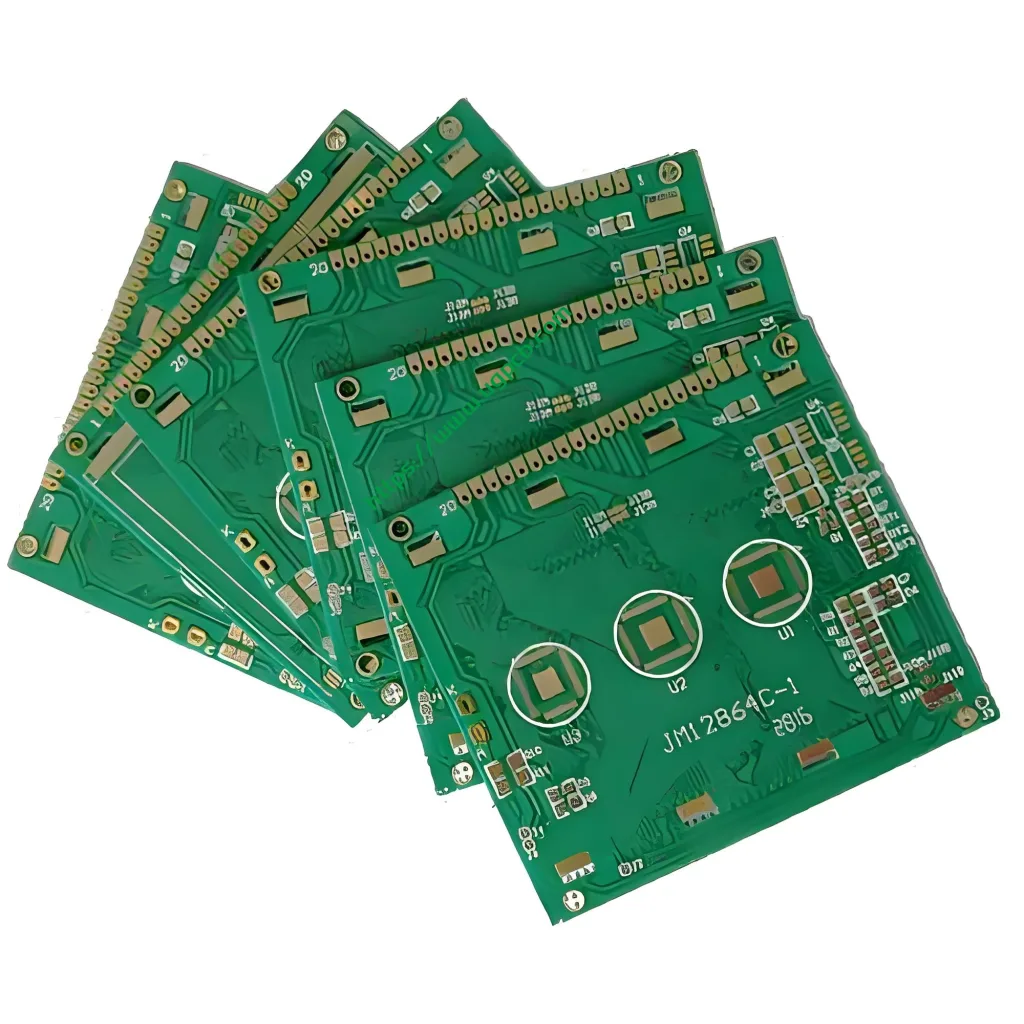
Définition du produit: What Is an LCD Liquid Crystal Display PCB?
Un PCB d'affichage à cristaux liquides LCD (Circuit imprimé) is a specialized circuit board designed for liquid crystal display driving systems. It performs three core functions: driving signal transmission, distribution d'énergie, and timing control signal routing. Unlike standard Cartes de circuits imprimés, un LCD display PCB demands tighter tolerances in line width precision, contrôle d'impédance, and surface flatness.
This product belongs to therigid double-sided PCB category with 2 couches (2L). It uses FR-4 grade flame-retardant material (UL 94 V-0 classé) and supports both SMT (Technologie de montage de surface) and through-hole component hybrid assembly processes. The board meets IPC-6012 Class 2 exigences de performance, making it suitable for industrial electronics and consumer electronics applications.
Spécifications de conception: Critical Parameters for LCD PCB Engineering
Matériau du substrat: The KB6165F Advantage
This product uses Kingboard KB6165F copper-clad laminate, which delivers the following key performance characteristics:
- Température de transition du verre (Tg): ≥150°C, ensuring dimensional stability during lead-free reflow soldering processes
- Température de décomposition thermique (Td): 325° C, providing excellent thermal reliability
- Cote d'inflammabilité: UL 94 V-0, with flame self-extinguishing within 10 seconds in vertical burn tests
- CTE (Coefficient de dilatation thermique): 12–15 ppm/°C in X-Y direction, 40–230 ppm/°C in Z direction, offering good thermal matching with LCD driver ICs
- FAC (Filament anodique conducteur) Résistance: Excellent anti-CAF performance ensuring long-term reliability
- Compatible sans plomb: Meets RoHS environmental requirements
According to IPC-2221 design standards, materials with Tg ≥150°C are suitable for lead-free assembly processes, capable of maintaining structural integrity under reflow soldering peak temperatures reaching 245–260°C.
Layer Count and Stack-up Design
The product features 2 couches (2L) with a standard 1.6 mm épaisseur du panneau. Pour IPC-2221, 1.6 mm represents the most commonly used thickness specification for rigid PCB, balancing mechanical strength with assembly convenience.
Line Width and Spacing Design
The minimum line width of 0.3 mm and minimum line spacing of 0.27 mm are carefully selected parameters forLCD driver PCB Intégrité du signal. Under IPC-2221 standards, the minimum spacing requirement for conventional voltage (≤30V) digital signal traces is 0.1 mm (4 mil). This product’s 0.27 mm (environ 10.6 mil) spacing far exceeds the IPC minimum requirement, providing ample margin for signal quality.
Design Calculation Reference (based on IPC-2221 outer layer conductor current-carrying capacity simplified formula):
Outer layer trace current-carrying capacity ≈ k × ΔT^0.448 × W^0.725 × T^0.725
Where k = 0.048 (for outer layer). At a 10°C temperature rise, un 0.3 mm trace with 1 oz copper thickness delivers a theoretical current-carrying capacity of approximately 1.2–1.5 A—sufficient for the power and signal trace requirements of conventional LCD driver boards.
Diamètre minimum du trou
The minimum hole diameter of 0.22 mm (environ 8.7 mil) falls within the precision drilling category. Under IPC-6012, the standard drilled hole diameter tolerance is ±0.08 mm (approximately ±3 mil) . Pour 0.22 micro-vias mm, manufacturing tolerances are typically controlled within ±0.05 mm.
Finition de surface: ENIG at 2U”
LeACCEPTER (Nickel chimique/Or par immersion) surface finish with 2U” épaisseur de l'or (environ 0.05 µm) complies with IPC-4552 requirements. IPC-4552 Revision A (issued in 2017) specifies gold deposit thickness of 0.04 μm à 0.10 µm (1.6 μin à 4.0 min) and nickel thickness of 3 μm à 6 µm.
Avantages de la finition de surface ENIG:
- Excellent solderability supporting multiple reflow cycles
- Strong wire bonding capability
- Superior oxidation and corrosion resistance
- Flat surface suitable for fine-pitch component mounting
- Extended shelf life
Principe de fonctionnement: Signal Transmission Mechanisms of the LCD Display PCB
LeLCD liquid crystal display PCB operates on two core functions: transmission de signaux etdistribution d'énergie.
1. Display Driver Signal Transmission: Display data from the main controller chip (MCU/SoC) travels through theCarte de circuit imprimé via microstrip or stripline traces to the LCD driver IC. The driver IC converts digital signals into analog grayscale voltages, which are then output through thePCB‘s fine traces to the ITO electrodes on the liquid crystal glass panel, controlling the twist angle of liquid crystal molecules to produce the displayed image.
2. Timing Control Signal Routing: LeLCD display PCB carries critical timing signals including VSYNC (Vertical Sync), HSYNC (Horizontal Sync), DCLK (Pixel Clock), and DE (Data Enable). The transmission delay and impedance matching of these signals directly affect display quality.
3. Power Management Distribution: LeLCD circuit board converts the input power (typiquement 3.3 V or 5 V) through DC-DC conversion circuits to generate the multiple voltage levels required by the LCD panel, including VGH (gate-on voltage, typiquement +15 V to +30 V), VGL (gate-off voltage, typically −5 V to −15 V), and AVDD (analog power voltage).
Classement du produit: LCD PCB Categories
LCD liquid crystal display PCBs peut être classé selon les dimensions suivantes:
Par nombre de couches
- Single-sided boards: Used for simple segment-code LCD displays
- Double-sided boards (2L): This product’s category, used for small to medium-sized TFT-LCD display drivers
- Panneaux multicouches (4L and above): Used for high-resolution, large-format display modules
Par finition de surface
- ENIG boards: This product’s category, offering the best overall performance
- OSP boards: Lower cost, suitable for short-lifecycle consumer electronics
- HASL boards: Suitable for LCD driver boards with wider pin pitches
Par candidature
- Consumer Electronics LCD PCBs: Smartphone secondary displays, smartwatch displays, e-reader screens
- Industrial Control LCD PCBs: Industrial HMI, instrument panel displays, CNC operation panel display drivers
- Automotive LCD PCBs: Systèmes d'infodivertissement embarqués, digital instrument clusters, HUD display control boards
- Medical Device LCD PCBs: Patient monitors, ultrasound diagnostic equipment, medical imaging system display driver boards
Core Performance Specifications
| Paramètre | Spécification | Norme de référence |
|---|---|---|
| Laminate Material | KB6165F (Planche King) | - |
| Type de stratifié | FR-4 Glass Fabric Copper-Clad Laminate | UL 94 V-0 |
| Nombre de couches | 2 couches (2L) | - |
| Épaisseur du panneau | 1.6 mm | CIB-2221 |
| Épaisseur de cuivre de la couche externe | 1 once (35 µm) | IPC-6012 Class 2 |
| Finition de surface | SEULEMENT 2U” (0.05 μm Au) | CIB-4552 |
| Nickel Layer Thickness | 3–6 μm (underlayer) | IPC-4552 Rev A |
| Diamètre minimum du trou | 0.22 mm | IPC-6012 |
| Largeur de ligne minimale | 0.3 mm | CIB-2221 |
| Espacement minimum des lignes | 0.27 mm | CIB-2221 |
| Dimensions de la carte | 147.2 × 65 mm | - |
| Tg (Température de transition du verre) | ≥150°C | - |
| Td (Température de décomposition thermique) | 325° C | - |
| CTE (X-Y Direction) | 12–15 ppm/°C | - |
| Cote d'inflammabilité | UL 94 V-0 | UL 94 |
| Résistance à l'arc | ≥60 seconds | - |
| Résistivité de surface | ≥2.6 × 10⁸ MΩ | - |
| Résistivité du volume | ≥3.4 × 10⁹ MΩ·cm | - |
Product Structure Analysis
LeLCD liquid crystal display PCB structure comprises the following layers from outside to inside:
1. Outer Layer – ENIG Surface Finish: Gold layer at 2U” (environ 0.05 µm) protects the underlying nickel layer from oxidation. The bottom nickel layer at 3–6 μm serves as a diffusion barrier between copper and gold.
2. Copper Foil Layer: 1 once (environ 35 µm) feuille de cuivre électrodéposée, etched to form the circuit pattern.
3. Dielectric Layer: FR-4 grade glass fabric impregnated with epoxy resin, environ 0.7 mm d'épaisseur (single layer), providing electrical insulation and mechanical support.
4. Copper Foil Layer: Couche inférieure 1 oz copper forming the bottom circuit pattern.
5. Outer Layer – ENIG Surface Finish: Symmetrical ENIG treatment matching the top layer.
Caractéristiques du produit: Why Choose UGPCB’s LCD Display PCB?
① High-Precision Manufacturing: Minimum hole diameter of 0.22 mm and minimum line width/spacing of 0.3 mm/0.27 mm support the routing requirements of high-density LCD driver boards.
② Premium Substrate Materials: Kingboard KB6165F high-end FR-4 material with Tg ≥150°C and UL 94 V-0 flammability rating ensures lead-free process compatibility and long-term reliability.
③ Standardized Surface Finish: SEULEMENT 2U” process complies with IPC-4552, delivering excellent solderability, résistance à l'oxydation, and extended shelf life.
④ Rigorous Quality Control: Products undergo full-process quality control per IPC-6012 Class 2 normes, covering hole diameter tolerance (±0.08 mm), hole copper thickness (≥20 μm), solder mask integrity, et tests électriques.
⑤ LCD-Optimized Design: Contrôle d'impédance, Intégrité du signal, and power integrity are optimized specifically for liquid crystal display driving applications.
Processus de fabrication: From Raw Material to Finished Product
UGPCB follows a rigorous standard manufacturing process forLCD display PCBs:
1. Découpe de matériaux →2. Inner Layer Pattern Transfer (drill positioning and registration marks) →3. Forage (minimum hole diameter 0.22 mm ± 0.08 mm) →4. Electroless Copper Deposition/Electroplating (hole metallization, hole copper thickness ≥20 μm) →5. Outer Layer Pattern Transfer (Largeur de ligne 0.3 mm / espacement 0.27 mm) →6. Placage de motifs (copper build-up to 1 once) →7. Gravure →8. Impression de masque de soudure →9. Finition de surface ENIG (ACCEPTER, gold thickness 2U”) →10. Profilage (dimensions 147.2 × 65 mm) →11. Tests électriques (100% essai électrique) →12. Inspection finale (Zone d'intérêt + inspection visuelle) →13. Emballage et expédition
Scénarios d'application typiques
📱 Consumer Electronics: Smartphone secondary displays, smartwatch displays, e-reader screen driver PCBs.
🏭 Industrial Control: PLC human-machine interfaces (HMI), industrial instrument displays, CNC operation panel display driver boards.
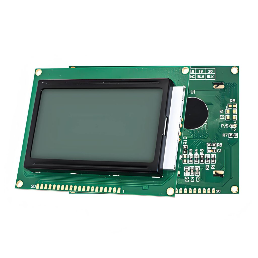
🚗 Automotive Electronics: Systèmes d'infodivertissement embarqués, digital instrument clusters, head-up display (ATH) display control PCBs.
🏥 Medical Devices: Patient monitors, ultrasound diagnostic equipment, medical imaging system display driver circuit boards.
🏠 Smart Home: Smart access control system displays, smart appliance control panels, building intercom system display module PCBs.
Pourquoi choisir UGPCB?
UGPCB brings years of LCD display PCB manufacturing experience to every project. We use premium raw materials like Kingboard KB6165F, strictly enforce IPC-6012 Class 2 normes de qualité, and operate high-precision drilling and circuit patterning equipment. Que vous ayez besoin Écran LCD Prototypage PCB or volume production, UGPCB delivers high-precision, high-reliability product solutions.
📞 Get Your LCD Display PCB Solution Today
UGPCB LCD liquid crystal display PCBs have been successfully deployed in numerous industrial, automobile, and consumer electronics display projects. Que vous ayez besoin LCD PCB prototyping for design validation or PCB turnkey assembly services, UGPCB provides full-process support from PCB fabrication to PCB Assemblage SMT.
Contact UGPCB’s professional team today for your custom LCD display PCB solution!
📧 E-mail: [info@ugpcb.com]
📞 Phone: [+86-755-XXXXXXXX]
🌐 Site Internet: [www.ugpcb.com]
Attribution de la source de données
The technical standards and data cited in this document are derived from the following authoritative sources:
- IPC-6012 -Qualification et spécifications de performances pour les cartes imprimées rigides – Defines PCB hole diameter tolerances (standard ±0.08 mm), hole copper thickness (Classe 2 ≥20 μm), and performance class requirements
- CIB-2221 -Norme générique sur la conception des cartes imprimées – Specifies line width/spacing design requirements and current-carrying capacity calculation formulas
- IPC-4552 Revision A (émis 2017) -Spécifications de performance pour le nickel chimique/l’or par immersion (ACCEPTER) Placage pour cartes imprimées – Specifies ENIG deposit thickness requirements: nickel 3–6 μm, gold 0.04–0.10 μm
- UL 94 -Norme de sécurité d'inflammabilité des matériaux plastiques pour les pièces des dispositifs et appareils –V-0 rating requires flame self-extinguishing within 10 secondes
- Kingboard KB6165F Product Datasheet – Substrate technical parameters (Tg ≥150°C, Td 325°C, UL 94 V-0, etc.)
- GB/T 4677 -Test Methods for Printed Boards – Used in conjunction with IPC standards as inspection references













