
Présentation du produit
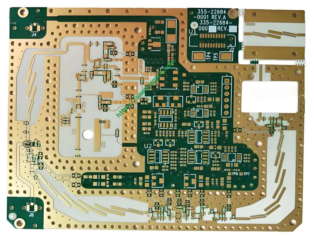
Le RO4350B + IT180 Mix Laminate High Frequency PCB Board represents an advanced engineered solution from UGPCB. This product combines Rogers RO4350B high-frequency material with IT180 epoxy laminate in a single 6-layer structure. It delivers excellent signal integrity for RF and microwave applications while optimizing manufacturing costs .
This hybrid construction uses Rogers RO4350B for critical high-frequency signal layers. IT180 provides mechanical support and handles digital/power distribution. The result is a high-performance board that meets the demanding requirements of modern communication systems.

Spécifications du produit
| Paramètre | Valeur |
|---|---|
| Modèle | RO4350B + IT180 Mix Laminate High Frequency PCB Board |
| Matériel | Rogers RO4350B + IT180 Mixing Press |
| Nombre de couches | 6 Calques |
| Constante diélectrique (NSP) | 3.48 |
| Épaisseur finie | 1.5 mm |
| Épaisseur du cuivre | 1 once (35 µm) |
| Contrôle de l'impédance | 50 ohm |
| Épaisseur diélectrique | 0.508 mm |
| Conductivité thermique | 0.69 W/m.k |
| Blind Hole Structure | 1L ~ 2L HDI |
| Traitement de surface | Immersion Or |
*Tableau: Complete technical specifications for UGPCB RO4350B+IT180 hybrid high frequency PCB*
What Is a Hybrid Laminate High Frequency PCB?
UN hybrid laminate PCB haute fréquence uses two or more different material types within a single board structure. This approach allows designers to place the right material in the right location based on electrical and mechanical requirements .
UGPCB’s 6-layer board features:
-
Rogers RO4350B on outer layers for high-frequency signal transmission
-
IT180 on inner layers for structural integrity and cost management
-
Precise impedance control à 50 ohm throughout all signal paths
This material combination leverages the strengths of each substrate while minimizing their individual limitations.
Material Properties and Performance
Rogers RO4350B Characteristics
RO4350B is a glass-reinforced hydrocarbon/ceramic laminate. It offers:
-
Constante diélectrique stable (NSP 3.48) across frequency and temperature
-
Low signal loss for RF and microwave applications
-
Consistent impedance control for 50 ohm designs
-
Excellent processability similar to standard FR-4 materials
-
Reliable performance up to 10 GHz and beyond
IT180 Laminate Characteristics
IT180 is a high-performance epoxy material with:
-
Température de transition de verre élevée (Tg 180°C)
-
Excellent thermal stability for lead-free assembly
-
Good mechanical strength and rigidity
-
Compatible CTE with RO4350B for reliable hybrid construction
-
Cost-effective solution for non-critical layers
Gestion thermique
The board achieves 0.69 W/m.k thermal conductivity. This ensures effective heat dissipation from power amplifiers and RF components. Proper thermal management extends product lifetime and maintains stable electrical performance under load .
Design Principles
Layer Stack-Up Strategy
The 6-layer construction follows these principles:
-
Couche 1-2: RO4350B material for high-frequency signal routing
-
Couche 3-4: IT180 for power distribution and ground planes
-
Couche 5-6: IT180 for additional signal routing and mechanical stability
This arrangement places RF signals close to the surface with controlled dielectric thickness of 0.508 mm. It provides optimal conditions for 50 ohm transmission line design .
HDI Blind Via Design
Les fonctionnalités du conseil 1L~2L IDH trous aveugles. These laser-drilled microvias:
-
Connect layer 1 directly to layer 2 without drilling through the entire board
-
Reduce signal path length for better high-frequency performance
-
Enable higher component density on the surface
-
Maintain signal integrity by minimizing via stubs
Contrôle de l'impédance
Précis 50 ohm contrôle d'impédance is maintained throughout all signal layers. This is achieved through:
-
Accurate dielectric constant (NSP 3.48) of RO4350B material
-
Controlled trace width and spacing based on 0.508 mm dielectric thickness
-
Consistent copper thickness of 1 once (35 µm)
-
Careful design of transitions and via structures
Principe de fonctionnement: How Materials Work Together
Signal Transmission in Hybrid Structures
High-frequency signals travel primarily on the outer layers where RO4350B is present. This material’s stable DK value of 3.48 ensures:
-
Consistent signal velocity across the board
-
Minimal phase distortion in RF paths
-
Reliable impedance matching for 50 ohm systems
-
Reduced insertion loss compared to standard materials
Thermal and Mechanical Roles
The IT180 layers serve critical support functions:
-
They provide mechanical rigidity to prevent board warpage
-
They conduct heat away from active components
-
They maintain dimensional stability during assembly
-
They offer cost savings without compromising RF performance
Layer-to-Layer Communication
Signals move between layers through:
-
Vias aveugles for high-frequency paths (L1-L2)
-
Buried vias for inner layer connections
-
Through-hole vias for power and ground distribution
This multi-level interconnect strategy preserves signal quality while enabling complex routing .
Processus de fabrication
Étape 1: Préparation des matériaux
RO4350B and IT180 laminates are cut to panel size. Copper foil and prepreg materials are prepared according to the stack-up design. All materials are baked to remove moisture before processing .
Étape 2: Imagerie de la couche interne
Inner layers are imaged with circuit patterns. Etching removes unwanted copper. Inspection optique automatisée (Zone d'intérêt) verifies pattern accuracy .
Étape 3: Laminage de la couche
RO4350B and IT180 layers are stacked in the correct sequence. Vacuum lamination applies heat and pressure. The hybrid materials bond together to form a single 6-layer structure. Precise temperature control prevents material separation .
Étape 4: Forage
Laser drilling creates 1L~2L blind vias with high precision. Mechanical drilling forms through-holes for other connections. Desmear processes clean all drilled holes .
Étape 5: Placage
Electroless copper deposits a thin conductive layer. Electrolytic copper plating builds up to 1 once (35 µm) épaisseur. This ensures reliable electrical connections through all vias .
Étape 6: Imagerie de la couche externe
Outer layers are imaged and etched. Final circuit patterns include fine-pitch features for modern components. AOI verifies outer layer quality .
Étape 7: Application du masque de soudure
Solder mask is applied to protect copper surfaces. It is imaged to expose pads for soldering. Thermal curing hardens the mask .
Étape 8: Finition de surface – Immersion Or
L'or d'immersion is applied to exposed copper areas. This finish provides:
-
Excellent solderability for assembly
-
Flat surface for BGA and fine-pitch components
-
Corrosion resistance for long-term reliability
-
Good performance for high-frequency skin effect
Étape 9: Tests électriques
100% electrical testing verifies:
-
Continuity of all nets
-
Isolation between nets
-
Impedance control at 50 ohm
-
No shorts or opens
Étape 10: Final Inspection and Packaging
Finished boards are visually inspected. They are vacuum-sealed with moisture barrier bags. Desiccant and humidity indicators are included for safe shipping .
![UGPCB technician inspecting hybrid PCB with immersion gold finish under magnification]
(Alt tag: Quality inspection of UGPCB RO4350B IT180 hybrid PCB with immersion gold surface finish)
Applications and Use Cases
Wireless Communication Equipment
This PCB is ideal for:
-
5Bornes de base G requiring stable RF performance
-
Radio frequency modules avec 50 ohm interface requirements
-
Wireless infrastructure operating at microwave frequencies
-
Antenna systems needing consistent dielectric properties
Radar
The board supports:
-
Automotive radar for ADAS applications
-
Millimeter-wave radar capteurs
-
Surveillance radar signal processing
-
Marine radar electronics requiring high reliability
High-Speed Data Transmission
Applications include:
-
Data center switches with high-speed SerDes interfaces
-
Network routers requiring signal integrity
-
Émetteurs-récepteurs optiques for telecommunications
-
High-performance computing interconnects
Aérospatial et défense
The material combination suits:
-
Communication par satellite subsystems
-
Avionics requiring thermal stability
-
Military radio équipement
-
Systèmes de navigation in extreme environments
Test et mesure
Typical uses:
-
RF test equipment interfaces
-
Spectrum analyzers front-end circuits
-
Signal generators output stages
-
Impedance analyzers test fixtures
Why Choose UGPCB’s Hybrid Solution?
Optimisation des coûts
Using RO4350B only where needed reduces material costs by 30-40% compared to full-RO4350B construction. IT180 provides mechanical strength at lower cost .
Performance Balance
The board delivers RF-grade performance on critical layers. It maintains standard material economy for non-critical sections. This balance suits modern mixed-signal designs .
Manufacturing Reliability
UGPCB’s hybrid lamination expertise ensures:
-
No delamination between dissimilar materials
-
Consistent impedance across all boards
-
Reliable HDI blind via connections
-
Flat, warp-free finished boards
Assurance qualité
-
100% electrical testing before shipment
-
Strict impedance control verification
-
Immersion gold for long-term reliability
-
Experienced engineering support
Classification
This product belongs to the following PCB categories:
| Classification Type | Catégorie |
|---|---|
| Par matériau | Organic resin-based high-frequency hybrid composite (Ceramic-filled hydrocarbon + High-Tg epoxy) |
| Par nombre de couches | 6-layer multilayer PCB |
| By Technology | IDH (Interconnexion à haute densité) avec 1-2 layer blind vias |
| Par candidature | RF/microwave communication PCB |
| By Surface Finish | Immersion Or (ACCEPTER) |
*Tableau: Scientific classification of UGPCB RO4350B+IT180 hybrid high frequency PCB*
Technical Data Summary
| Paramètre | Valeur | Condition |
|---|---|---|
| Constante diélectrique (NSP) | 3.48 | À 10 GHz |
| Facteur de dissipation (DF) | 0.0037 | À 10 GHz, RO4350B |
| Conductivité thermique | 0.69 W/m.k | Z-direction |
| Température de transition du verre | >280° C (RO4350B) / 180° C (IT180) | TMA method |
| Coefficient de dilatation thermique | 30-40 ppm/°C | X/Y direction |
| Résistance à l'écoulement | >1.05 N/mm | 1 cuivre oz |
| Moisture Absorption | 0.06% | RO4350B, 24-hour immersion |
| Cote d'inflammabilité | UL 94 V-0 | Both materials |
| Maximum Processing Temperature | 250° C | Lead-free assembly compatible |
Tableau: Comprehensive technical data for RO4350B and IT180 hybrid construction
Frequently Asked Questions
Q: What is the main advantage of using hybrid materials?
UN: Hybrid construction places RO4350B only on high-frequency layers. This reduces material costs while maintaining RF performance. IT180 provides mechanical strength at lower cost .
Q: Can this board support 50 ohm impedance requirements?
UN: Oui. The board is designed for strict 50 ohm impedance control. Dielectric thickness of 0.508 mm and DK 3.48 enable precise trace width calculations .
Q: What is the purpose of HDI blind vias?
UN: 1L~2L blind vias connect the top layer directly to layer 2. This shortens signal paths and improves high-frequency performance. It also enables higher component density .
Q: Is immersion gold suitable for high-frequency applications?
UN: Oui. Immersion gold provides excellent surface flatness. It supports the skin effect at high frequencies. It also offers long shelf life and good solderability .
Q: What is the thermal conductivity value?
UN: The board achieves 0.69 W/m.k thermal conductivity. This helps dissipate heat from power amplifiers and RF components .
Q: How does this compare to full RO4350B construction?
UN: This hybrid approach costs 30-40% less than full RO4350B. It maintains RF performance on critical layers. Mechanical strength is actually improved by IT180’s rigidity .
Ordering Information
UGPCB offers complete support for your hybrid PCB requirements:
-
Quick Turnaround: Prototype quantities in 10 working days
-
Volume Production: Consistent quality for mass production runs
-
Engineering Support: DFM feedback before manufacturing
-
Quality Guarantee: 100% electrical test, impedance verified
How to Order
-
Send your Gerber files to UGPCB
-
Specify RO4350B + IT180 hybrid construction
-
Indicate 6-layer, 1.5 mm épaisseur, 1 cuivre oz
-
Request 50 ohm impedance control and 1L-2L HDI blind vias
-
Choose immersion gold surface finish
-
Receive engineering review within 24 heures
-
Approve and begin production
Get Your Quote Today
Ready to start your next high-frequency project with UGPCB?
Our team of RF PCB specialists is ready to assist you. We provide:
-
Free DFM analysis
-
Competitive pricing for prototypes and production
-
Fast turnaround times
-
Expert technical support
[Contact Our Engineering Team]
E-mail: sales@ugpcb.com
Website: www.ugpcb.com
UGPCB – Your Trusted Partner for High Frequency Hybrid PCB Solutions


