

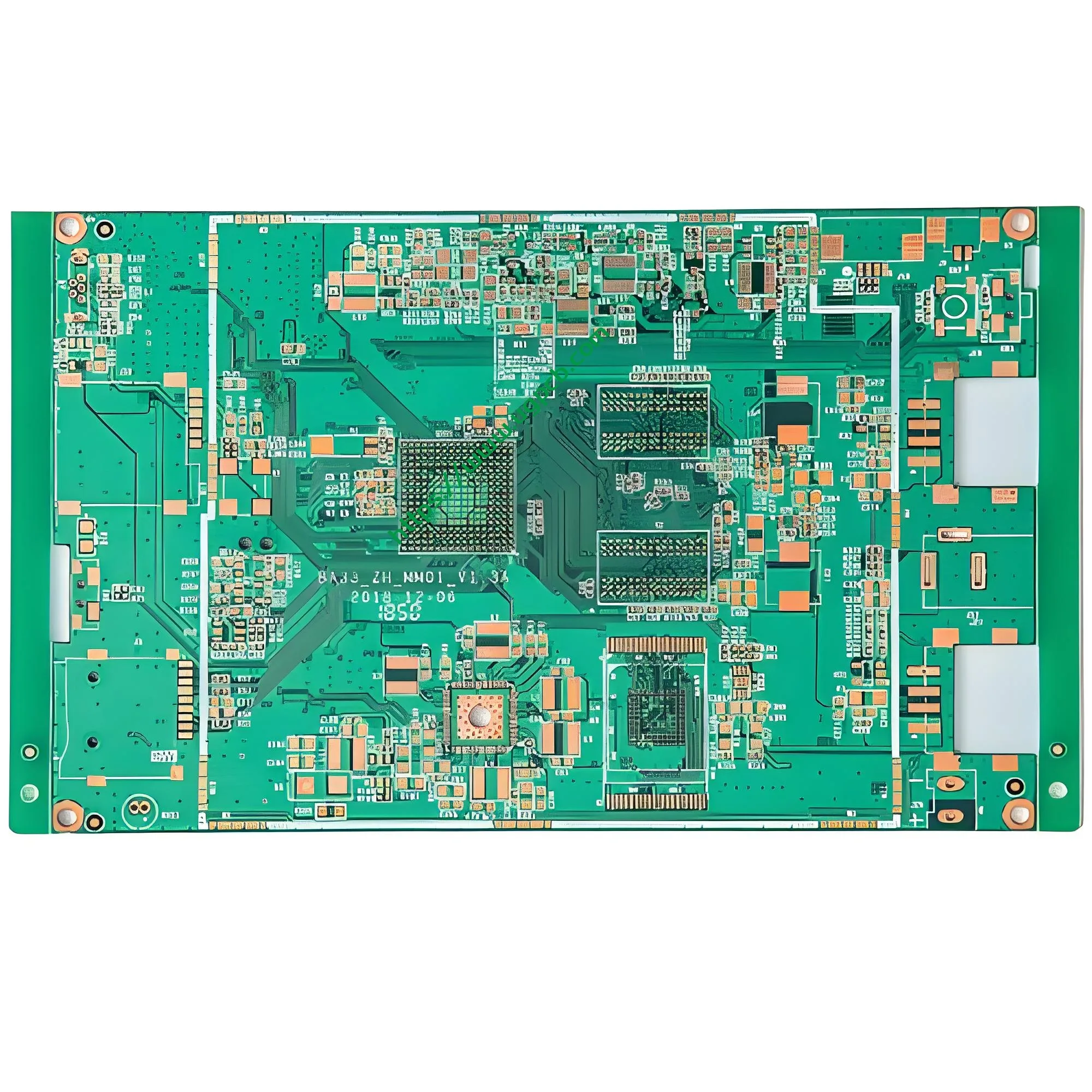
Présentation du produit: Qu'est-ce qu'une carte de circuit imprimé antioxydant OSP?
UnCarte PCB antioxydante OSP utiliseConservateurs de soudabilité organique (OSP) comme sa finition de surface en cuivre. Ce processus dépose un film organique ultra-mince sur les surfaces de cuivre nues. Le film empêche l'oxydation pendant le stockage et le montage. Pendant le soudage, le flux dissout rapidement le film OSP. Cela expose du cuivre propre pour des joints de soudure fiables.
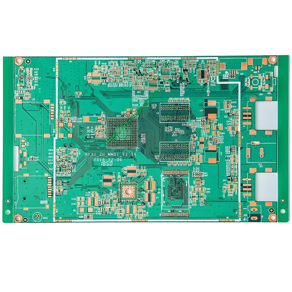
La carte de circuit imprimé antioxydant OSP de l'UGPCB utiliseStratifié époxy verre FR-4 comme matériau de base. Il comporte 35μm (1 once) feuille de cuivre, 1.6mm épaisseur du panneau, et les dimensions de 68.36 × 34,6 mm. La taille minimale du trou fini est de 0,45 mm. La largeur minimale des traces est de 0,15 mm et l'espacement minimum est de 0,20 mm.. Le produit est entièrement conforme à IPC-6012E (qualification et performances des cartes imprimées rigides) et IPC-4555 (performances OSP à haute température) caractéristiques.
CePCB OSP double face sert l'électronique grand public, équipement de communication, et contrôles industriels. Il fonctionne mieux là où la sensibilité aux coûts et la planéité de la surface comptent le plus..
Classification scientifique des produits
Basé sur les systèmes internationaux de classification des PCB, ce produit entre dans ces catégories:
| Dimension de classification | Catégorie |
|---|---|
| Matériau du substrat | PCB rigide en tissu de verre époxy FR-4 |
| Nombre de couches | Double face (circuit à deux couches) |
| Finition de surface | OSP (Conservateurs de soudabilité organique) antioxydant |
| Cote d'inflammabilité | UL 94 V-0 |
| Classe de performances IPC | Classe 2 (produits électroniques de service dédié) |
| Épaisseur de la feuille de cuivre | 1 once (35µm) cuivre standard |
| Épaisseur du panneau | 1.6panneau rigide standard de mm |
| Type de trou | Trou traversant compatible avec SMT |
Paramètres techniques clés expliqués
Substrat: Tissu de verre époxy FR-4
FR-4 est le substrat rigide le plus courant dans le PCB industrie. “FR” signifie ignifuge. “4” indique une résine époxy combinée à un tissu de verre qui répondUL 94 V-0 normes d'inflammabilité. UL 94 V-0 nécessite que les spécimens verticaux s'auto-éteignent à l'intérieur10 secondes après deux applications de flamme de 10 secondes. Aucune goutte enflammée ne peut enflammer le coton.

La température de transition vitreuse (Tg) mesure la résistance à la chaleur. La norme FR-4 Tg varie de 130 à 140°C. La moyenne Tg FR-4 atteint 150-160°C. Le FR-4 à haute Tg dépasse 170°C. Ce produit utilise la norme FR-4 avec Tg ≥ 130°C (Conforme à la norme IPC-4101/21). Cela répond aux exigences de choc thermique du brasage par refusion (températures maximales 240–260°C).
Épaisseur de la feuille de cuivre: 35µm (1 once)
L'épaisseur du cuivre détermine la capacité de transport de courant. Ce produit utilise35µm feuille de cuivre, connu sous le nom1 cuivre oz (1 oz/pi² ≈ 35μm). Selon IPC-2221, 1 once de cuivre à une élévation de température de 10°C porte environ:
- 0.15mm (6 mil) largeur de trace: 0.5-0,7A
- 0.20mm (8 mil) largeur de trace: 0.8-1,0A
L'épaisseur de cuivre de 35 μm est la norme la plus courante pour les PCB double face. Il équilibre les coûts, capacité actuelle, et rendement de fabrication.
Dimensions de la carte: 68.36 × 34,6 mm
La planche finie mesure68.36mm × 34,6 mm. Cette taille compacte convient aux modules électroniques étroits. Les petits circuits imprimés exigent une précision plus stricte : les tolérances dimensionnelles restent généralement inférieures à ± 0,15 mm. (Classe IPC-6012 2).
Taille minimale du trou fini: 0.45mm
0.45mm est le trou traversant plaqué minimum (PTH) diamètre. Cette taille de trou est une norme dans l'industrie. Il garantit un placage fiable (rapport hauteur/largeur environ 3.6:1 avec une épaisseur de panneau de 1,6 mm). La taille du trou s'adapte à la plupart des composants DIP et des conceptions de plots SMT standard.
Épaisseur du PCB: 1.6mm
1.6mm est l'épaisseur de carte la plus courante dans la fabrication de PCB. Il offre une excellente résistance mécanique et rigidité à la flexion. Il s'adapte parfaitement aux connecteurs et prises standards.
Largeur de trace et espacement: 0.15mm / 0.20mm
Ce produit offrelargeur de trace minimale de 0,15 mm (à propos 6 milles) etespacement minimum de 0,20 mm (à propos 8 milles). Selon la classification IPC, ces dimensions entrent dansClasse 2 (produits électroniques de service dédié). Cette précision répond à la plupart des conceptions de PCB à densité moyenne, y compris les cartes de contrôle MCU, modules de gestion de l'énergie, et cartes de conversion d'interface.
Comment fonctionne le processus antioxydant OSP
Le processus OSP produit un film organique ultra-fin sur du cuivre nu et propre.adsorption chimique. Le film OSP se compose principalement decomposés d'alkylbenzimidazole (à base d'azole). L'épaisseur du film varie généralement de0.2–0,5μm.
Mécanisme de protection
Le film OSP protège les surfaces en cuivre grâce à trois mécanismes:
- Barrière physique – Le film organique forme une couche moléculaire dense. Il empêche l'oxygène et l'humidité d'entrer en contact avec la surface du cuivre..
- Adsorption chimique – Les groupes actifs des molécules OSP se lient chimiquement aux atomes de cuivre. Cela crée une forte adhérence.
- Protection sélective – Le film OSP couvre uniquement les zones en cuivre. Cela n'affecte pas le masque de soudure ou d'autres régions non métalliques.
Comportement pendant le soudage
Pendant la refusion SMT, les températures atteignent190–230°C. Les principes actifs du flux décomposent et dissolvent le film OSP. Cela expose du cuivre propre en dessous. La soudure entre directement en contact avec le cuivre nu et formecomposés intermétalliques (Imc). Cela crée des connexions électriques fiables. Le film OSPse décompose complètement sans résidu après soudure.
Caractéristiques de performance clés
Basé sur les méthodes de test IPC-TM-650:
| Caractéristiques | Valeur typique / Exigence | Norme de référence |
|---|---|---|
| Épaisseur du film OSP | 0.2–0,5μm | CIB-4555 |
| Angle de mouillage de la soudure | ≤30° (après 1 reflux) | IPC-TM-650 2.4.1 |
| Rapport de propagation de la soudure | ≥80% | IPC-TM-650 2.4.1 |
| Protection contre l'oxydation (ambiant) | ≥6 mois | CIB-4555 |
| Changement de résistance de contact | ≤10% (après 6 mois de stockage) | IPC-TM-650 |
Processus de fabrication de PCB antioxydants OSP
La fabrication de PCB antioxydants OSP suit des contrôles de processus stricts. Chaque étape affecte la qualité finale et la fiabilité.
Processus frontaux (Préparation du substrat & Modèle de circuit)
- Découpe de matériaux – Couper le stratifié cuivré FR-4 aux dimensions voulues
- Forage – Perçage CNC avec une taille de trou minimale de 0,45 mm
- Cuivre chimique / Galvanoplastie – Métalliser les parois des trous pour une connexion couche à couche
- Transfert de modèle de circuit – Film sec / exposition et développement d'un film humide
- Gravure – Supprimez le cuivre indésirable pour créer une trace de 0,15 mm / 0.20circuits d'espacement en mm
- Impression de masque de soudure – Appliquez de l’encre de masque de soudure verte ou d’une autre couleur
- Pré-nettoyage – Éliminer les oxydes et les contaminants avant la finition de surface
Processus de revêtement OSP (Processus de base)
Le flux typique de revêtement OSP:
Dégraissage → Double rinçage à l'eau → Micro-gravure → Double rinçage à l'eau → Décapage à l'acide → Rinçage à l'eau DI → Formation de film OSP → Séchage à l'air → Rinçage à l'eau DI → Séchage final
- Micro-gravure – Élimine les oxydes de cuivre et crée une surface uniforme et microscopiquement rugueuse. Cela favorise la croissance du film OSP.
- Formation de films OSP – Plonger le PCB dans la chimie OSP (alkylbenzimidazole, acides organiques, chlorure de cuivre, et eau déminéralisée). Le film se développe par adsorption chimique sur les surfaces en cuivre.
- Contrôle de l'épaisseur du film – Un contrôle précis est essentiel. Trop fin signifie une mauvaise résistance à la chaleur. Une épaisseur trop épaisse entrave l’action du flux et l’écoulement de la soudure.
Processus back-end
- Routage – Routage CNC aux dimensions finales
- Tests électriques – Test de sonde volante ou de montage
- Inspection finale – Inspection visuelle et échantillonnage de l’épaisseur du film
- Emballage sous vide – Emballage résistant à l’humidité et à l’oxydation
Caractéristiques du produit et principaux avantages
Excellente planéité de la surface
Le film OSP est seulement0.2–0,5μm épais. Il se forme par adsorption chimique avec une épaisseur uniforme et une surface lisse. Cela préserve la planéité originale de la feuille de cuivre. C'est idéal pourSMT à pas fin composants (tels que 0,4 mm et un pas QFP inférieur, Forfaits QFN).
Soudabilité supérieure
Le film OSP se dissout rapidement dans le flux lors de la refusion. Cela expose du cuivre frais pour une formation IMC fiable. Le processus OSP prend en charge à la foistraversant (Tht) etmontage en surface (CMS) soudure.
Rentable
OSP n'utilise aucun métal précieux (or, argent, palladium). Les coûts de matériaux et de traitement sont inférieurs à ceux d'ENIG, argent par immersion, ou une boîte à immersion. Pour la production en grand volume comme l'électronique grand public, OSP offre une compétitivité-coût exceptionnelle.
Respectueux de l'environnement
OSP utilise des composés organiques. Il ne contient pas de plomb, mercure, cadmium, ou chrome hexavalent. Il répond pleinementRoHS 2.0 exigences. Les coûts et la complexité du traitement des déchets sont également inférieurs à ceux des processus de finition des métaux.
Temps de traitement court
Le revêtement OSP est simple et rapide. Il ne nécessite aucun équipement de placage complexe ni de longs temps de dépôt. Par rapport à ENIG (ce qui prend des heures), OSP termine la finition de surface en30–60 minutes par lot. Cela réduit considérablement les délais de livraison.
Directives de conception et considérations importantes
Conception pour la fabrication (DFM) Règles
Basé sur les capacités de processus de ce produit:
| Paramètre de conception | Capacité du produit | Valeur de conception recommandée |
|---|---|---|
| Largeur de trace minimale | 0.15mm | ≥0,15 mm (traces de signaux) |
| Espacement minimal | 0.20mm | ≥0,20 mm |
| Taille minimale du trou | 0.45mm | ≥0,45 mm |
| Épaisseur du panneau | 1.6mm | 1.6mm (standard) |
Limites et atténuations du processus OSP
OSP offre de nombreux avantages mais présente des limites inhérentes:
- Durée de conservation limitée – Le film OSP protège6 mois dans des conditions ambiantes. Pour une meilleure soudabilité, assemblage SMT complet dans 3 mois.
- Sensibilité à l'humidité – Les films OSP se dégradent à haute température, environnements très humides. Rangez les planches à20–25 °C avec 40 à 60 % d'humidité relative.
- Cycles de refusion limités – La norme OSP résiste1–2 chocs thermiques de refusion. Les refusions multiples nécessitent un OSP à haute température (Conforme IPC-4555).
- Défis des tests électriques – Le film OSP est isolant. Cela affecte la fiabilité des contacts de test électrique. Les points de test nécessitent une impression de pâte à souder pour supprimer la couche OSP.
Recommandations de stockage et de manipulation
- Emballage sous vide avec cartes déshydratantes et indicateurs d'humidité
- Environnement de stockage: température ≤30°C, humidité relative ≤60%
- Soudure complète à l'intérieur48 heures d'ouvrir le colis
- Porter des gants antistatiques lors de la manipulation. Évitez tout contact des mains nues avec les surfaces des planches.
Scénarios d'application typiques
Les cartes de circuits imprimés antioxydantes OSP servent de nombreuses industries en raison de leuravantage de coût, planéité de la surface, et une excellente soudabilité:
Electronique grand public
- Cartes mères de smartphones et PCB de tablettes
- Cartes mères et cartes graphiques d'ordinateur
- Tableaux de commande d'appareils électroménagers
- Cartes de circuits imprimés pour appareils portables
Équipement de communication
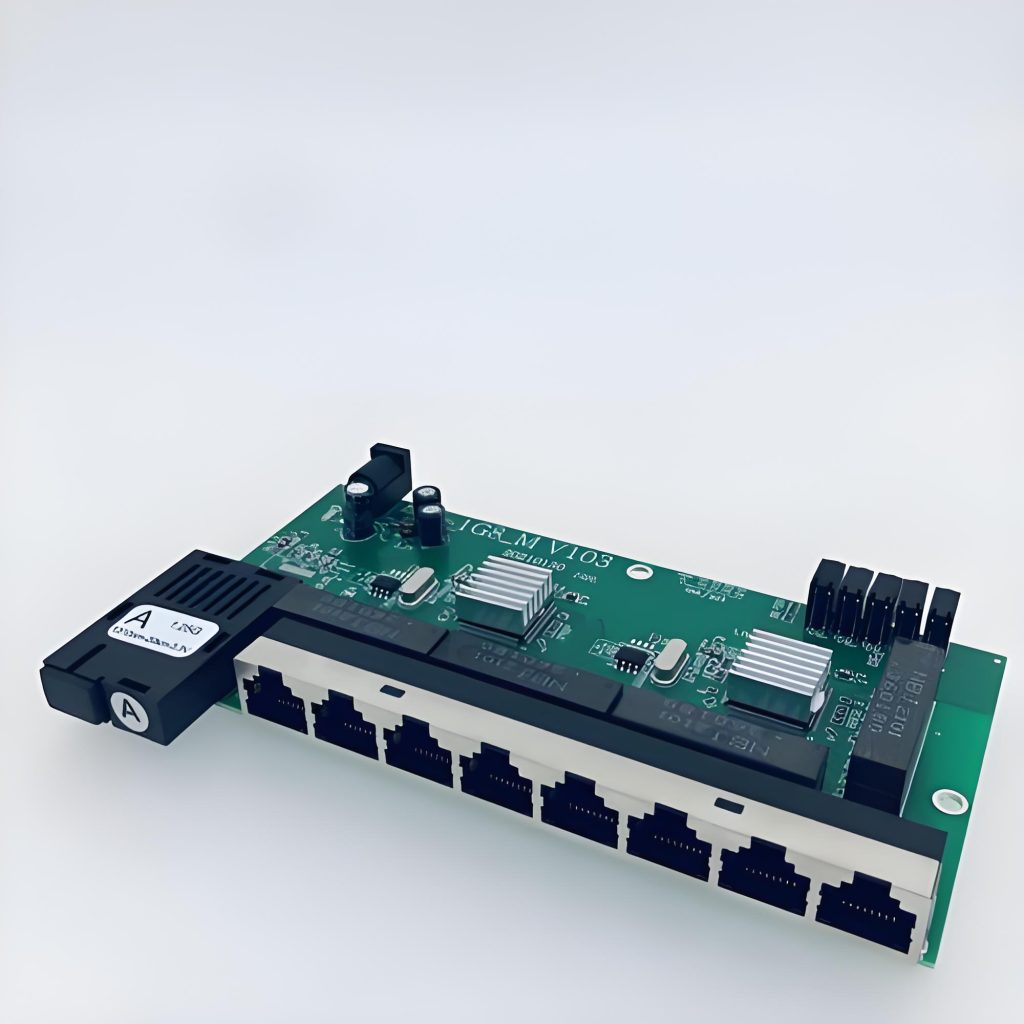
- PCB de routeur et de commutateur
- Modules de communication et appareils IoT
- Bluetooth / Cartes porteuses de modules Wi-Fi
Commandes industrielles
- Contrôleurs logiques programmables PLC
- Modules de gestion de l'alimentation
- Cartes de circuits imprimés d'instrumentation
- Cartes de commande d'entraînement de moteur
Électronique automobile (Non critique pour la sécurité)
- Systèmes d'infodivertissement embarqués
- Modules de contrôle du corps
- Cartes d'interface de capteur
Assurance qualité et conformité aux normes
Normes applicables
Le produit PCB antioxydant OSP de l'UGPCB suit strictement ces normes internationales:
| Standard | Titre | Portée |
|---|---|---|
| CIB-4555 | Spécifications de performance pour les conservateurs organiques de soudabilité à haute température (OSP) pour cartes imprimées | Exigences et tests du processus OSP |
| IPC-6012E | Qualification et spécifications de performances pour les cartes imprimées rigides | Qualité et performances du panneau fini |
| IPC-4101/21 | Spécification pour le stratifié époxy renforcé de verre | Exigences techniques du substrat FR-4 |
| IPC-TM-650 | Manuel des méthodes d'essai | Diverses méthodes de tests de performances |
| UL 94 V-0 | Inflammabilité des matières plastiques | Sécurité ignifuge du substrat |
| RoHS 2.0 | Restriction des substances dangereuses | Conformité environnementale |
Indicateurs clés de qualité
Selon les exigences IPC, les indicateurs de qualité clés incluent:
- Épaisseur du film OSP: 0.2–0,5μm, tolérance d'uniformité ≤ ±0,1 μm
- Adhésion: ≥4B (IPC-TM-650 2.4.29 essai transversal)
- Rapport de propagation de la soudure: ≥80% (IPC-TM-650 2.4.1)
- Période de protection contre l'oxydation: ≥6 mois (conditions ambiantes)
- Cote d'inflammabilité: UL 94 V-0
Pourquoi choisir l'UGPCB pour les PCB antioxydants OSP?
Capacités de fabrication de précision
- 0.15mm largeur de trace minimale / 0.20mm espacement minimum
- 0.45mm taille minimale du trou fini
- 1.6mm d'épaisseur de panneau standard avec une excellente compatibilité
Contrôle fiable du processus OSP
- Respect strict de la norme IPC-4555 pour l'épaisseur et la qualité du film
- Traçabilité complète tout au long du processus de fabrication
- Tests de soudabilité et échantillonnage de l'épaisseur du film pour chaque lot
Livraison rapide
- Délai de livraison standard: 7–10 jours ouvrés
- Prend en charge à la fois l'échantillonnage de prototypes et la production en volume
Support technique complet
- Examen gratuit de la conception DFM
- Équipe d'ingénierie professionnelle pour des conseils de sélection de produits
Obtenez un devis aujourd'hui
UGPCB propose des solutions de circuits imprimés antioxydants OSP de grande valeur. Que vous ayez besoinéchantillonnage de prototypes ouproduction en volume, nous fournissons un support technique professionnel et des prix compétitifs.
📞 Comment obtenir un devis:
- Soumettez vos fichiers Gerber et votre liste de nomenclatures
- Notre équipe d'ingénierie répond avec une solution personnalisée et un devis dans les délais24 heures
- Vérification DFM gratuite pour garantir que votre conception réussit du premier coup
Déclaration de source de données: Les données techniques et les exigences standard citées dans ce document sont principalement dérivées de l'IPC (Association reliant les industries électroniques) normes dont IPC-4555 “Spécifications de performance pour les conservateurs organiques de soudabilité à haute température (OSP) pour cartes imprimées,” IPC-6012E “Qualification et spécifications de performances pour les cartes imprimées rigides,” IPC-4101/21 “Spécification pour le stratifié époxy renforcé de verre,” IPC-TM-650 “Manuel des méthodes d'essai,” et UL 94 “Norme pour les tests d'inflammabilité des matériaux plastiques pour les pièces d'appareils et d'appareils.” Certains paramètres de processus font référence à des données techniques accessibles au public provenant des principaux fabricants de PCB.. Toutes les données ont été vérifiées pour leur exactitude.













