

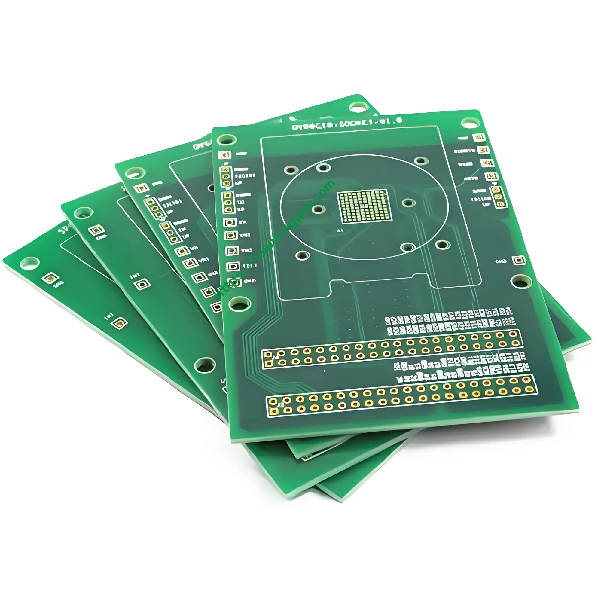
1. Présentation du produit: What Is a Wireless Vacuum Cleaner PCB?
A wireless vacuum cleaner PCB (Circuit imprimé) is the core electronic component responsible for motor drive control, gestion de l'énergie, user interaction, and safety protection inside a cordless vacuum cleaner. In simple terms, it serves as the “brain” and “nerve center” of the device. It receives button commands, controls brushless motor speed, manages battery charging and discharging, monitors operating status, and implements multiple safety protections.
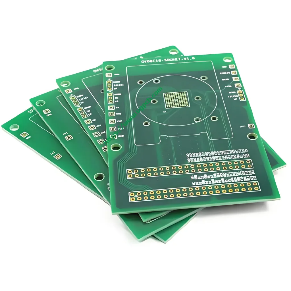
UGPCB introduces this Wireless Vacuum Cleaner PCB – a 2-layer rigid printed circuit board designed specifically for portable cleaning equipment. It uses FR-4 glass epoxy copper-clad laminate comme matériau de base. The board thickness is 1.0mm, and the dimensions are 86.37 × 72.6mm. This compact size fits perfectly into the tight internal spaces of handheld and stick-style cordless vacuums.
Selon IPC-6012F Qualification et spécifications de performances pour les cartes imprimées rigides, this product falls under the rigid double-sided printed board (with plated-through holes) catégorie. As a key part of UGPCB’s one-stop PCB solutions, this product meets IPC international standards from design through manufacturing and quality control. It provides vacuum cleaner manufacturers with a high-reliability, rentable PCB solution.
2. Classement du produit: Scientific Positioning and Industry Categorization
Per IPC-6012F and PCB standard industry classification systems, ce produit peut être scientifiquement classé comme suit:
| Dimension de classification | Catégorie |
|---|---|
| Par structure | Rigid double-sided printed board (with plated-through holes) |
| Par matériau de base | FR-4 epoxy woven glass copper-clad laminate (compliant with IPC-4101) |
| Par nombre de couches | 2-panneau de couches (PCB double face) |
| Par finition de surface | HASL sans plomb (Nivellement de la soudure à air chaud) |
| Par indice d'inflammabilité | UL 94 V-0 |
| Par candidature | Électronique grand public / small appliance control board (vacuum cleaner PCBA) |
Within the vacuum cleaner electronics industry, this product belongs to themotor drive and control PCBA catégorie. Together with the main control board and power management board, it forms the three core circuit modules of a wireless vacuum cleaner.
3. Paramètres techniques clés
3.1 Base Material and Board Thickness
- Matériau de base: FR-4 (glass fiber reinforced epoxy copper-clad laminate)
- Épaisseur du panneau: 1.0mm
FR-4 is the most widely used rigid substrate in the PCB industry. Pour IPC-4101, FR-4 offers excellent electrical insulation, résistance mécanique, et résistance à la chaleur. Standard FR-4 has a glass transition temperature (Tg) of 130–140°C. Pour IPC-6012, the tolerance range for 1.0mm board thickness is ±0.1mm.
3.2 Nombre de couches et dimensions
- Nombre de couches: 2 couches (tableau double face)
- Dimensions: 86.37 × 72.6 mm
The 2-layer structure effectively controls manufacturing cost while delivering solid electrical performance. This makes it the mainstream choice for wireless vacuum cleaner control boards. The compact 86.37 × 72.6mm dimensions are optimized for the limited space inside vacuum cleaners.
3.3 Trace Width/Spacing and Minimum Hole Size
- Taille minimale du trou: 0.45mm
- Largeur de trace / espacement: 0.45mm / 0.391mm
Selon IPC-2221CNorme générique sur la conception des cartes imprimées, trace width and spacing design must consider electrical performance, current-carrying capacity, and manufacturing capability. The 0.45mm minimum hole size supports reliable soldering of conventional DIP components and through-hole parts.
For current-carrying capacity, the industry-standard formulaI = k·ΔT^0.44·A^0.725 (where A is the trace cross-sectional area) shows that with 1oz copper, a 0.45mm (environ. 18mil) trace can carry about 1.8–2.0A. The wireless vacuum cleaner PCB uses this trace width for motor drive signals and control signals, ensuring long-term stable operation.
3.4 Épaisseur de la feuille de cuivre
- Épaisseur de la feuille de cuivre: 1/1 once (1 ounce on both outer layers)
1feuille de cuivre d'une once (environ. 35µm) is the standard configuration for consumer electronics PCBs. It strikes an excellent balance between current-carrying capacity, conductivité thermique, et coûter.
3.5 Finition de surface
- Finition de surface: HASL sans plomb (Nivellement de la soudure à air chaud)
HASL is a mature and economical PCB surface finish. Lead-free HASL meets RoHS environmental requirements. Par normes IPC, lead-free HASL typically has a tin layer thickness of 1–40μm, with conventional processes控制在 5–25μm. This finish offers excellent solderability (wettability) and a good storage life of up to 12 mois.
3.6 Masque de soudure et légende
- Couleur du masque de soudure: Green ink
- Couleur de la légende: Blanc
Green solder mask is the industry’s most popular choice. It provides excellent insulation protection and high contrast for Zone d'intérêt (Inspection optique automatisée). White legends are clear and easy to read, facilitating component placement and future maintenance.
4. Directives de conception: Following IPC-2221C Standards
A well-designed wireless vacuum cleaner PCB must follow these core principles (per IPC-2221C):
4.1 Electrical Performance Design
- Power Trace Width: Calculate using the formula I = k·ΔT^0.44·A^0.725 to ensure temperature rise stays below 10°C at maximum operating current.
- Intégrité du signal: Use 0.45mm trace width for control signals to guarantee complete transmission of PWM speed control signals and sensor signals.
- Grounding Design: Use single-point grounding or split grounding strategies to prevent power loop interference with the control loop.
4.2 Conception de gestion thermique
Wireless vacuum cleaners generate significant heat from MOSFETs during operation. Le Conception de circuits imprimés must address this by:
- Placing thermal via arrays under power devices.
- Widening high-current traces or adding exposed copper for better heat dissipation.
- Using 1.0mm board thickness to balance thermal conductivity and mechanical strength.
4.3 Mechanical Structure Design
Le 86.37 × 72.6mm dimensions must precisely match the vacuum cleaner housing. Mounting hole positions and connector locations must meet structural design requirements. The 0.45mm minimum hole size supports through-hole soldering for various DIP components and connectors.
5. Principe de fonctionnement
The wireless vacuum cleaner PCB operates through the following core processes:
① Power Input and Management: The lithium battery pack (typically 21.6V or 25.2V) passes through the power management circuit on the PCB. This provides stable voltages to the main control chip and driver circuits.
② Main Control Chip Computation: The MCU (microcontrôleur) on the PCB receives button commands. It calculates and outputs three-phase drive signals using FOC (Contrôle orienté champ) or square-wave control algorithms.
③ Motor Drive: The drive signals are amplified by MOSFET power devices. These signals then drive the brushless DC motor (BLDC) to rotate at high speed, generating the airflow needed for suction.
④ Feedback and Protection: The PCB continuously monitors motor current, battery voltage, température, and other parameters. When it detects abnormal conditions such as overcurrent, overtemperature, undervoltage, or rotor lock, it immediately executes protection actions.
6. Matériaux utilisés
| Composant | Matériel | Description |
|---|---|---|
| Substrat | FR-4 glass epoxy | Compliant with IPC-4101 |
| Conductive Layer | Electrolytic copper foil (1once) | 1oz sur les deux couches extérieures |
| Masque de soudure | Green photoimageable ink | Insulation protection, résistance à l'oxydation |
| Finition de surface | Lead-free HASL alloy | Rohs conforme |
| Encre de légende | White epoxy ink | High contrast, heat resistant |
FR-4 substrate carries a UL 94 V-0 cote d'inflammabilité. Dans le test de brûlure verticale, the flame extinguishes within 10 seconds after removal, with no burning drips. This feature is critical for high-power, battery-powered devices like wireless vacuum cleaners. It significantly reduces the risk of fire caused by circuit faults.
7. Spécifications de performance
7.1 Performance électrique
| Paramètre | Spécification | Norme de référence |
|---|---|---|
| Résistance d'isolation | ≥10^6 MΩ | IPC-6012F |
| Tension de tenue diélectrique | Up to 500V (design-dependent) | IPC-2221C |
| Conduction Resistance | ≤50mΩ (typique) | IPC-6012F |
| Impédance caractéristique | Controllable on request (50Ω/90Ω/100Ω) | IPC-2221C |
7.2 Performance thermique
| Paramètre | Spécification | Norme de référence |
|---|---|---|
| Température de transition du verre (Tg) | ≥135°C (Méthode DSC) | IPC-TM-650 2.4.25 |
| Solder Heat Resistance | 288° C / 10s, pas de délaminage | CIB-4101 |
| Axe Z CTE (CTEz) | ≤65 ppm/°C (50–260°C) | CIB-4101 |
7.3 Performances mécaniques
| Paramètre | Spécification | Norme de référence |
|---|---|---|
| Board Thickness Tolerance | ±0.1mm | IPC-6012 |
| Hole Size Tolerance | ± 0,05 mm | IPC-6012F |
| Cote d'inflammabilité | UL 94 V-0 | UL 94 |
7.4 Fiabilité
- Test de soudabilité: Compliant with IPC-J-STD-003
- Aging Test: 500 hours under double-85 conditions (85° C / 85%Rh) with no abnormalities
8. Caractéristiques structurelles
8.1 2-Layer Board Advantages
The top layer carries the main components and signal traces. The bottom layer handles auxiliary components and ground/power copper pours. The 2-layer design achieves thebest cost ethighest reliability balance for wireless vacuum cleaner control functions.
8.2 Trou traversant plaqué (PTH) Processus
All through-holes use the plated-through hole process. This ensures reliable interconnection between top and bottom layers. It also provides solid mechanical support and electrical connection for DIP components.
8.3 Solder Mask Bridge Process
Green solder mask forms bridges between adjacent pads. This prevents soldering shorts and improves SMT placement yield.
9. Flux de processus de fabrication
UGPCB strictly follows IPC-6012F standards to control every production step:
① Incoming Material Inspection →② Inner Layer Circuit Creation (for 2-layer boards, this is directly the outer layer) →③ Lamination (not applicable for 2-layer boards) →④ Drilling (minimum hole size 0.45mm) →⑤ Electroless Copper Deposition / Placage de panneaux →⑥ Outer Layer Circuit →⑦ Pattern Plating →⑧ Etching →⑨ Solder Mask (green ink) →⑩ Surface Finish (HASL sans plomb) →⑪ Legend (white characters) →⑫ Profile Routing (86.37 × 72.6mm) →⑬ Electrical Test →⑭ Final Inspection (per IPC-A-600) →⑮ Packaging and Shipping
Every batch undergoestest de sonde volante oudedicated fixture testing pour assurer 100% no open or short circuits.
10. Scénarios d'application
10.1 Applications principales
- Handheld cordless vacuums: Motor drive and control in compact spaces
- Stick-style cordless vacuums: Battery management and brushless motor drive
- Robot vacuums: Navigation control and motor drive
- Car vacuums: 12V/24V power adaptation and control
- Smart cleaning devices: IoT connectivity and intelligent control
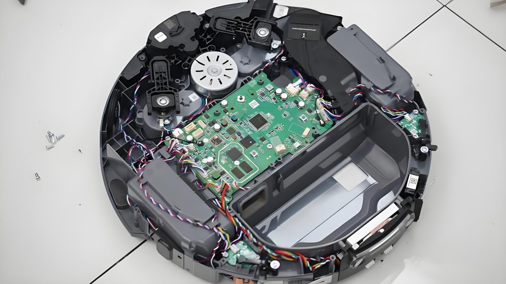
10.2 End-Product Examples
This PCB can be widely used in control boards and driver boards for cordless vacuums and similar cleaning devices from brands such as Xiaomi, Dyson, Tineco, and Leifheit.
11. Why Choose UGPCB’s Wireless Vacuum Cleaner PCB?
✅International Standards Compliance: Conception, fabrication, and inspection fully comply with IPC-6012F, IPC-A-600, IPC-2221C, et d'autres normes internationales
✅UL94V-0 Fire Safety: FR-4 substrate achieves the highest vertical burn rating, ensuring device safety

✅Lead-Free Eco-Friendly Process: Lead-free HASL surface finish meets RoHS and REACH environmental directives
✅Proven Manufacturing Capability: UGPCB provides one-stop services from PCB design and manufacturing to PCBA assembly
✅Strict Quality Control: Visual inspection per IPC-A-600 and 100% electrical testing ensure shipment quality
✅Compact Optimized Dimensions: Le 86.37 × 72.6mm size perfectly fits the internal space of various wireless vacuum cleaners
12. Obtenez un devis et des échantillons aujourd'hui
UGPCB is committed to providing high-precision, high-reliability PCB and PCBA solutions to electronics manufacturers worldwide. Que vous ayez besoin bare PCBs, fully assembled PCBA, ou one-stop services from design to mass production, UGPCB has the expertise to support you.
📧Contact UGPCB for a custom quote today →
- Site web: www.ugpcb.com
- Custom design modifications and optimizations available
- Free DFM (Conception de la fabrication) revoir
- Quick-turn prototyping and volume production both available
Déclaration de source de données
The technical standards and data cited in this article come from the following authoritative organizations:
- IPC (Association reliant les industries électroniques): IPC-6012F Qualification et spécifications de performances pour les cartes imprimées rigides, IPC-A-600 Acceptabilité des cartes imprimées, IPC-2221C Norme générique sur la conception des cartes imprimées, CIB-4101 Spécification des matériaux de base pour les cartes imprimées rigides et multicouches, IPC-TM-650 Manuel des méthodes d'essai
- UL (Laboratoires souterrains): UL 94 Norme de sécurité d'inflammabilité des matériaux plastiques pour les pièces des dispositifs et appareils –V-0 notation
- Industry Standard Engineering Formula: PCB current-carrying capacity formula I = k·ΔT^0.44·A^0.725













