

In the era of data-intensive and ultra-high-speed signal transmission, a Printed Circuit Board (PCB) is far more than a simple component carrier; it is the critical architecture defining system performance limits. For demanding applications like high-speed networking, artificial intelligence computing, and advanced test instrumentation, standard FR-4 materials fall short. UGPCB addresses this need with our advanced 22-layer multilayer PCB built on Panasonic Megtron-6 R-5775G laminate, engineered to meet challenges of high frequency, low loss, and complex interconnectivity.
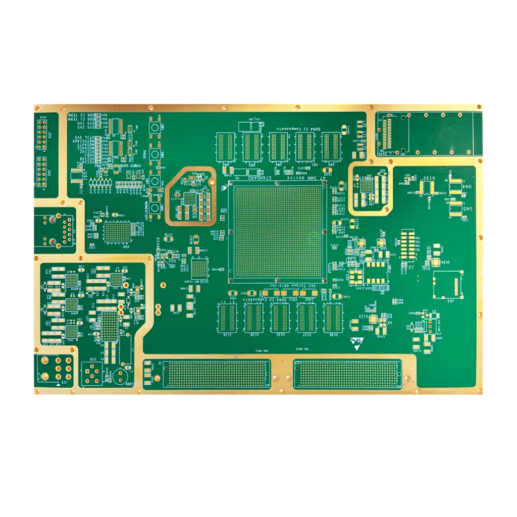
1.UGPCB’s 22-Layer Megtron-6 High-Speed PCB Présentation du produit & Définition
This product is a 22-layer High-Density Interconnect (IDH) rigid printed circuit board. Its core advantage lies in the use of a premium-grade, grande vitesse, low-loss laminate—Panasonic’s Megtron-6 R-5775G. Combined with a robust 2.0mm board thickness and precision lamination technology, it creates a high-end interconnection platform capable of handling high-frequency signals above 10GHz with exceptional signal integrity and power integrity.

2. Critical Design Considerations
Designing such an advanced carte de circuit imprimé multicouche requires focus on:
-
Contrôle de l'impédance: Precise calculation and control of single-ended and differential impedance to ensure consistent signal propagation within the Megtron-6 dielectric.
-
Optimisation du stack-up: The intelligent arrangement of the 22 conductive layers (22Calques)—including signal, pouvoir, and ground planes—is crucial for maximizing shielding and minimizing crosstalk in this high-layer count PCB.
-
Gestion thermique: The 2.0mm board thickness and multilayer structure aid heat distribution. Cependant, strategic use of thermal vias remains essential for high-power IC areas.
-
High-Frequency Routing: Employing microstrip or stripline configurations, avoiding acute angle turns, and leveraging the low-profile copper foil of Megtron-6 to reduce losses from skin effect.
3. How It Works & Structure
UN PCB’s primary function is to provide electrical connectivity and signal transmission between components via etched copper traces on an insulating substrate. Ce 22-carte PCB de couche structure resembles a precise “multi-layer sandwich”:
-
Couches intérieures: Use H/HOZ (environ 1/1 oz or 35µm) copper for core power, avions de sol, and some internal signal routing.
-
Outer Layers: Utiliser 1/1 oz copper for mounting primary components and routing critical signal traces.
-
Dielectric Layers: All insulating prepreg materials are Panasonic Megtron-6 R-5775G, whose low Dielectric Constant (Ne sait pas) et facteur de dissipation (Df) ensure superior high-speed signal transmission.
-
Finition de surface: Or par immersion au nickel autocatalytique (ACCEPTER) à 2 micro-inches (2toi”). This provides a flat, solderable surface, excellent oxidation resistance, and good wire-bonding capability, ideal for high-density BGA packages and RF connectors.
4. Core Material: Panasonic Megtron-6 R-5775G
This is the heart of this advanced PCB material. Megtron-6 is Panasonic’s next-generation, grande vitesse, low-loss circuit board material series.
-
Key Performance: Features an extremely low Dielectric Constant (Dk~3.5) and ultra-low Dissipation Factor (Df~0.0015 @ 10GHz), significantly outperforming standard FR-4. Its high Glass Transition Temperature (Tg) ensures superior thermal stability and dimensional consistency during high-temperature reflow soldering processes.
-
Application Fit: Optimized for high-speed digital signals (10Gbps+ to 56/112Gbps) and millimeter-wave RF applications.
| Article | Méthode d'essai | Condition | Unité | Megtron6 R-5775(N) Tissu de verre à faible Dk |
Megtron6 R-5775 Tissu de verre normal |
|
| Température de transition vitreuse.(Tg) | DSC | UN | ° C | 185 | 185 | |
| Température de décomposition thermique.(Td) | TGA | UN | ° C | 410 | 410 | |
| Axe X CTE | a1 | IPC-TM-650 2.4.24 | UN | ppm/°C | 14-16 | 14-16 |
| Axe Y CTE | 14-16 | 14-16 | ||||
| Axe z CTE | a1 | IPC-TM-650 2.4.24 | UN | 45 | 45 | |
| a2 | 260 | 260 | ||||
| T288(avec du cuivre) | IPC-TM-650 2.4.24.1 | UN | min | >120 | >120 | |
| Constante diélectrique(Ne sait pas) | 12GHz | Type équilibré résonateur à disque circulaire |
C-24/23/50 | - | 3.4 | 3.6 |
| Facteur de dissipation(Df) | 0.004 | 0.004 | ||||
| Absorption d'eau | IPC-TM-650 2.6.2.1 | J-24/23 | % | 0.14 | 0.14 | |
| Module de flexion | Remplir | JISC 6481 | UN | GPA | 18 | 19 |
| Résistance au pelage* | 1once(35µm) | IPC-TM-650 2.4.8 | UN | kN/m | 0.8 | 0.8 |
5. Caractéristiques clés & Performance
-
Ultra-Low Signal Loss: Megtron-6 material ensures maximum efficiency in high-frequency signal transmission with minimal attenuation.
-
Excellent Thermal & Dimensional Stability: High Tg value combined with a 2.0mm thick board suits high-temperature, high-power application environments.
-
High-Density Interconnect Capability: The 22-layer design provides abundant routing channels, supporting complex interconnections for large-scale chips (par ex., FPGA, GPUs).
-
Precise Impedance & Layer-to-Layer Registration: Mature manufacturing processes guarantee consistent electrical performance across the carte PCB multicouche.
-
Superior Solderability & Bonding: The 2u” ENIG finish ensures highly reliable solder joints and is suitable for precision SMT assembly.
6. Scientific Classification & Applications principales
-
Scientific Classification:
-
Par nombre de couches: High Multilayer PCB (Typiquement >10 couches).
-
Par matériau: PCB à grande vitesse / PCB haute fréquence / Low-Loss PCB.
-
By Technology: PCB HDI (Subject to specific design features like blind/buried vias).
-
By Rigidity: PCB rigide.
-
-
Applications principales & Cas d'utilisation:
-
High-Speed Networking Equipment: Core backplanes and motherboards for 400G/800G optical modules, high-end routers, and switches.
-
Advanced Computing & Stockage: AI server boards, Informatique haute performance (HPC) clusters, enterprise SSD controller boards.
-
Aérospatial & Radar: RF front-ends and signal processing units for avionics communication and phased array radar systems.
-
Advanced Test & Measurement Instruments: Mainboards within high-speed oscilloscopes, spectrum analyzers, and signal generators.
-
7. Production Flow Overview
UGPCB adheres to a stringent PCB manufacturing process to ensure quality:
Material Cutting → Inner Layer Imaging → Lamination (22-Alignement des calques & Bonding) → Drilling → Hole Metallization → Outer Layer Imaging → Pattern Plating → Etching → Solder Mask Application → ENIG Surface Finish → Routing / Scoring → Electrical Testing → Final Inspection (AOL)
Every step is supported by high-precision equipment, with multiple quality control checkpoints integrated into the PCB fabrication process, ensuring this 22-layer Megtron-6 PCB meets the highest standards from design to delivery.
Don’t let base materials limit your innovative designs.
Whether you’re developing next-gen communication hardware or tackling frontier computing challenges, UGPCB 22-layer high-performance PCB solution is your reliable hardware foundation. We provide not just a product, but full-spectrum support from PCB design consultation to rapid prototyping and volume production.
Click to request a quote and receive expert technical documentation. Power your project with a superior core!


