
Engineered for the Edge of Innovation
The evolution toward bezel-less displays and multi-lens camera systems in smartphones, coupled with the demand for miniaturization in medical endoscopy, presents a universal challenge: every millimeter of internal space saved translates to significant design gains. Traditional rigid PCB cannot bend, while flexible circuits (FPC) often lack adequate support in component-dense areas.
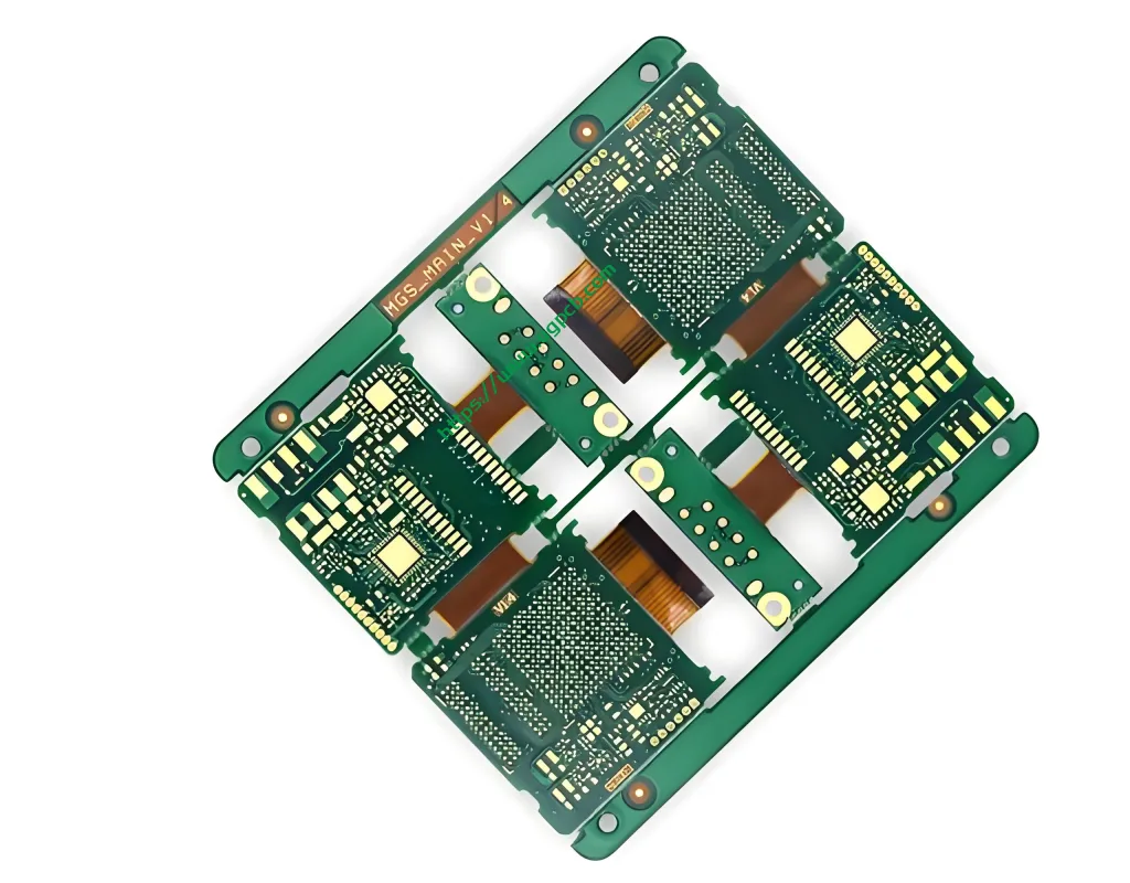
UGPCB introduces its advanced PCB du module de caméra rigide-flex, a solution that masterfully combines the mechanical stability of FR-4 with the dynamic flexibility of polyimide (PI). This innovative interconnect eliminates connectors and harnesses, providing a direct, fiable, and space-efficient link for compact camera systems.

1. Présentation du produit: Defining the Rigid-Flex Camera Module PCB
UN PCB rigide-flexible is not a simple assembly of a rigid board and a flexible cable connected by a connector. It is a monolithic, inseparable structure formed by laminating thin, flexible polyimide substrates with robust FR-4 epoxy glass-reinforced cores through advanced vacuum lamination processes .
UGPCB’s offering is specifically engineered for modules de caméra. It features a 2-layer rigid + 2-layer flexible construction. This design replaces bulky connectors and cables found in traditional setups, drastically shortening the signal path between the CMOS image sensor and the main application processor.
2. Principes de conception: The Art of Balancing Stiffness and Flexibility
Designing this type of PCB requires precise 3D planning to balance electrical performance with mechanical endurance. UGPCB’s engineering focuses on several critical aspects:
-
Stack-up Architecture: The design employs a symmetrical construction with a rigid section thickness of 0.4mm et un flexible section thickness of just 0.15mm. This precise control ensures that during bending, the neutral axis of the flexible region aligns with the copper conductor, significantly reducing stress and preventing trace fracture.
-
Transition Zone Management: The interface between rigid and flexible areas is the product’s most critical zone. UGPCB utilizes controlled adhesive flow techniques and via plugging to prevent delamination or stress concentration during repeated flexing cycles.
-
Intégrité du signal: To handle high-speed data from modern image sensors, the design adheres to strict impedance control, facilitated by a minimum trace/space of 3mil/3mil. This ensures clean signal transmission, free from noise or interference that could degrade image quality.
3. Matériels & Performance: Built on a Foundation of Quality
The exceptional performance of this PCB stems from a rigorous selection of premium materials:
-
Rigid Layer Material: High-grade FR-4 provides the necessary mechanical strength. It guarantees absolute flatness for mounting the CMOS sensor, a non-negotiable requirement for maintaining the precise focal plane of the camera module.
-
Flexible Layer Material: Polyimide (PI) film is the industry standard for the flexible layers . PI offers exceptional heat resistance (withstanding lead-free reflow profiles), outstanding flexural endurance for both static and dynamic bending applications, and excellent chemical stability.
-
Finition de surface: The PCB features an Nickel électrolaire à l'immersion du palladium électrolaire (Énipique) finition. This advanced surface treatment deposits layers of nickel, palladium, et de l'or . It provides a perfectly flat surface, excellent solderability for miniature components, and is ideal for aluminum or gold wire bonding, which is often required in sensor packaging .
4. Spécifications clés
The following parameters demonstrate UGPCB’s capability in high-precision, miniaturized manufacturing:
-
Modèle: PCB du module de caméra rigide-flex
-
Combinaison de matériaux: FR-4 (Rigide) + PI (Flex)
-
Configuration de la couche: Rigide 2 Calques / Flex 2 Calques
-
Couleur du masque de soudure: Vert / Blanc (Optional)
-
Épaisseur finie: Rigid Area 0.4mm / Flex Area 0.15mm
-
Poids du cuivre: 1 once (environ. 35µm)
-
Minimum Line Width/Space: 3mil / 3mil
-
Traitement de surface: Énipique (NiPdAu)
-
Primary Application: PCB du module de caméra (for smartphones, automobile, médical, drones)
5. Comment ça marche: Structure and Functionality
Structurellement, this PCB can be visualized as a “rigid island” floating on a “flexible sea.”
-
Rigid Zone: The thicker (0.4mm) FR-4 areas serve as the mounting platform for the image sensor and passive components. This rigidity ensures that during auto-focus or optical image stabilization, the solder joints connecting the sensor are not subjected to mechanical stress.
-
Flexible Zone: The ultra-thin (0.15mm) PI-based areas act as a ribbon cable, routing high-speed image data from the rigid island to the main logic board. Its thin profile allows it to be folded into tight Z-shapes or U-shapes, conforming perfectly to the limited space inside a smartphone, drone, or endoscopic camera.
-
Principe opérationnel: When light hits the camera sensor, the generated electrical signals travel through the precision-etched copper traces within the flexible zone. The integrity of these signals is maintained by the impedance-controlled design, ensuring the final image is sharp and free from artifacts.
6. Processus de fabrication: A Journey of Precision
UGPCB follows industry-leading processes, aligned with IPC standards, to ensure each rigid-flex PCB meets the highest reliability standards :
-
Préparation des matériaux & Cleaning: FR-4 and PI base materials are cut to size. The PI material undergoes plasma treatment to enhance surface energy, ensuring strong adhesion during lamination.
-
Imagerie de la couche interne: Using photolithography, the fine 3mil circuits are etched onto both rigid and flexible layers. Inspection optique automatisée (Zone d'intérêt) verifies the absence of defects like opens or shorts .
-
Laminage & Vacuum Bonding: The prepared inner layers are stacked with bonding sheets (préampe) and laminated under high temperature and pressure in a vacuum environment. This process fuses the rigid and flexible sections into a single, inseparable unit without unwanted adhesive bleed .
-
Forage & Placage: Mechanical and UV laser drilling create micro-vias for layer interconnection. These holes are then made conductive through electroless copper plating and reinforced with electroplated copper.
-
Couche externe & Finition de surface: The outer circuit layers are formed, followed by the application of the Énipique finition de surface.
-
Coverlay Application & Profiling: A protective polyimide coverlay is applied. Laser cutting is then used to precisely “ouvrir” the coverlay over pads and to profile the final board shape, ensuring zero mechanical stress on the delicate flex areas .
7. Classement scientifique
Selon les normes de l'industrie, this product is classified as:
-
Par structure: Multilayer Rigid-Flex Printed Circuit Board (specifically a 2R+2F construction).
-
Par candidature: Optoelectronic Module PCB (Module caméra).
-
Par technologie: IDH PCB rigide-flexible, due to its fine 3mil trace width and microvia requirements.
8. Applications: Beyond the Smartphone
While optimized for camera modules, the attributes of this PCB make it ideal for a range of demanding applications:
-
Electronique grand public: Multi-camera modules in flagship smartphones, cameras in foldable devices, and ultra-slim laptop webcams.
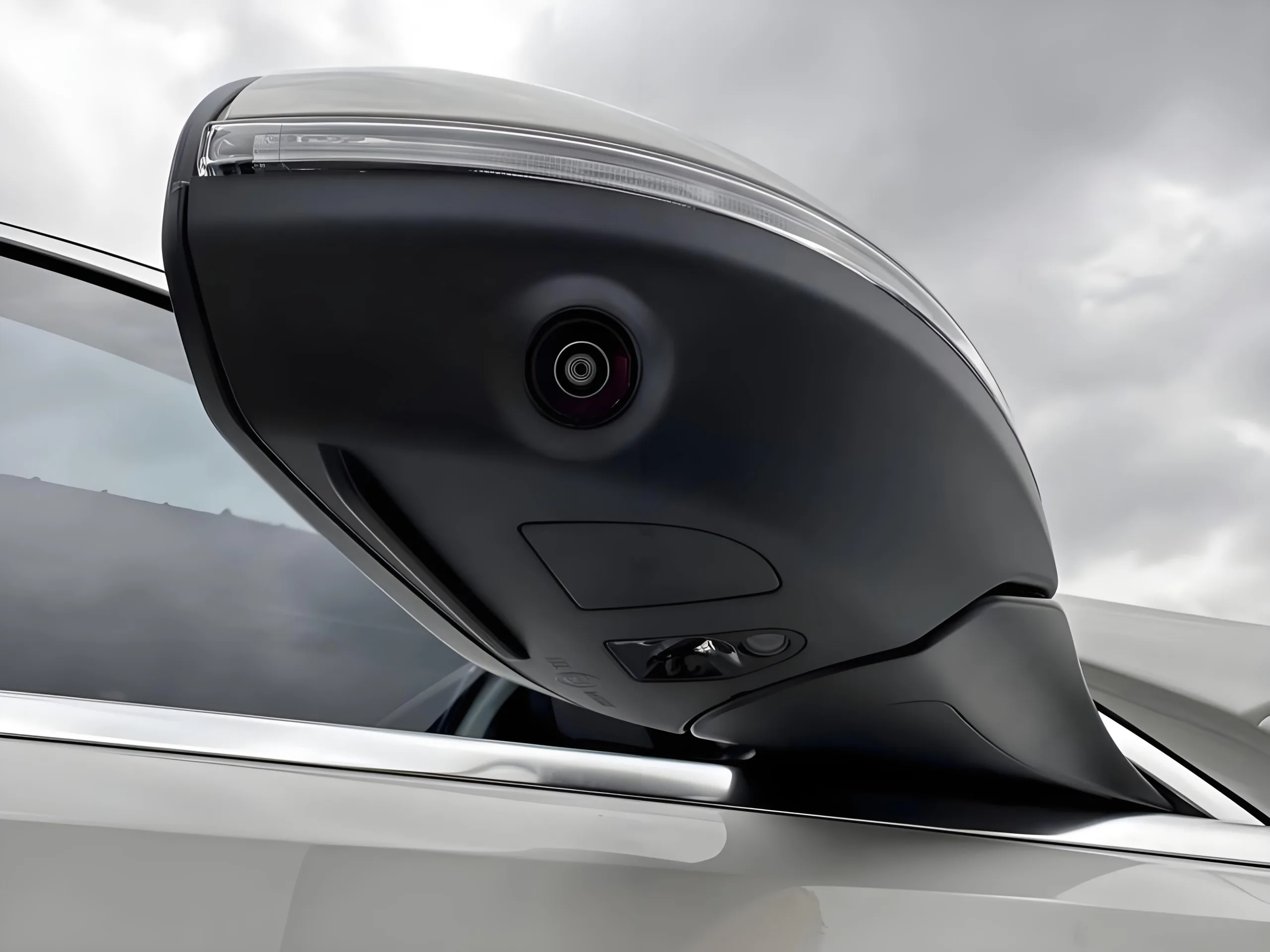
-
Électronique automobile: 360-degree surround-view cameras and Driver Monitoring Systems (DMS). These environments demand reliability under extreme vibration and temperature fluctuations (-40°C to +85°C), where rigid-flex boards eliminate the risk of connector failure.
-
Dispositifs médicaux: Miniature endoscopes and imaging probes. The combination of extreme thinness and high reliability allows for insertion into small cavities while transmitting high-definition video.
9. Why Partner with UGPCB for Your Camera Module Needs?
-
Unlock Space: The combination of a 0.4mm rigid zone and a 0.15mm flexible zone can save over 60% of the space compared to traditional “board-to-cable” interconnect solutions.
-
Enhance Reliability: By eliminating connectors and solder joints, the failure rate in high-vibration environments can be reduced by up to 70%.
-
Guarantee Signal Fidelity: Precision 3mil/3mil lines ensure stable transmission channels for high-speed interfaces like MIPI, preserving image integrity from sensor to processor.
Get a Quote and Empower Your Next-Gen Product
UGPCB is more than a manufacturer; we are a partner in innovation. Whether you are developing a flagship smartphone or a cutting-edge medical imaging device, notre PCB du module de caméra rigide-flex is engineered to meet your most demanding requirements for space, poids, et fiabilité.
Send your Gerber files or design inquiries to [sales@ugpcb.com] . Our engineering team will provide a professional DFM (Conception de la fabrication) analysis and a competitive volume quote within 24 heures. Choose UGPCB for precision you can rely on.


I don’t commonly comment but I gotta say regards for the post on this special one : D.